ZX81 ULA Replacement.
By Andy Rea.
April / May 2007.
The aim of this project is to build a ZX81 ULA
equivalent circuit using discrete components that are readily available. No modification to the ZX81 circuit board should be
allowed, and the only connections between the ZX81 and the ULA replacement
should be the 40 pins of the original ULA socket. So to start I need to
understand the function and mode of operation of each of the 40 ULA pins. This
information is just my opinion and findings it may contain errors or omissions
and is used at your own risk.
Pin Function Function Pin
1 A7' +5V 40
2 A8' A6' 39
3 A2' A5' 38
4 A1' A4' 37
5 A0' A3' 36
6 /RD OSC 35
7 /IORQ GND 34
8 /WR KBD0 33
9 /MREQ D0 32
10 /M1
KBD1 31
11 A14
D1 30
12 /RAMCS
KBD2 29
13 /ROMCS D2 28
14 /CLK
KBD3 27
15 /NMI
D3 26
16 TV-TAPE KBD4 25
17 /HALT D4 24
18 A15
D5 23
19 D7
UK/US 22
20 TAPE
IN
D6 21
A little further explanation of each group
of pins.
Power and ground.
-----------------
Pin 34 = Ground ( 0v )
Pin 40 = Vcc ( +5v )
Not really anything important to know
about this.
Port $FE input group.
---------------------
Pin 20 = tape input (bit
7)
Pin 22 = uk/us select (bit
6)
Pin 25 = kbd4 (bit
4, keyboard columns 5,6)
Pin 27 = kbd3 (bit
3, keyboard columns 4,7)
Pin 29 = kbd2 (bit
2, keyboard columns 3,8)
Pin 31 = kbd1 (bit
1, keyboard columns 2,9)
Pin 33 = kbd0 (bit
0, keyboard columns 1,0)
The more astute person may notice that bit 5 is
missing; in my design I have used a pull-up resistor on this bit so it always
returns logic 1.
The tape input (pin 20) is connected to a simple
filter circuit.
The uk/us select is left open circuit in a UK machine
and shorted to 0v (or to 0v via a low value resistor), since there is no
pull-up resistor on the ZX81 circuit board one is provided in the ULA
replacement design.
Kdb0 thru kdb4 pins 33,31,29,27,25 respectively
These are the keyboard columns connected to the 5way
keyboard connector, there are pull up resistors on the ZX81 circuit board for
these inputs so no special precautions are needed.
Control input group.
--------------------
Pin 6 = /RD (direct
to CPU /RD)
Pin 7 = /IORQ (direct
to CPU /IORQ)
Pin 8 = /WR (direct
to CPU /WR)
Pin 9 = /MREQ (direct
to CPU /MREQ)
Pin 10 = /M1 (direct
to CPU /M1)
Pin 11 = A14 (direct
to CPU A14)
Pin 17 = /HALT (direct
to CPU /HALT)
Pin 18 = A15 (direct
to CPU A15)
/MREQ (pin 9) used in conjunction with A14 (pin 11) to
generate the /ROMCS and /RAMCS outputs.
/MREQ A14 /ROMCS /RAMCS
0 0 0 1
0 1 1 0
1 0 1 1
1 1 1 1
The /ROMCS signal is simply -
/MREQ
OR'd with A14.
The /RAMCS signal is almost as simple -
/MREQ
OR'd with (NOT A14)
/RD (pin 6) and /WR (pin 8) are used by the ULA in
conjunction with /IORQ to control the internal control ports. There are
basically 4 internal ports, 2 that control the VSYNC signal (that is also the
tape output signal), and 2 that control the NMI generator.
PORT $FE (writing to port OUT ($FE),A) turns on the
NMI generator, this port is not fully decoded so any
OUT ($xx),A with bit 0 of the port address low, will
turn the NMI generator on.
PORT $FD (writing to port OUT ($FD),A) turns off the
NMI generator, this port is not fully decoded so any
OUT ($xx),A with bit 1 of the port address low, will
turn the NMI generator off.
IF you were to execute the instruction OUT ($FC),A you
would effectively be trying to turn the NMI generator on and off at the same
time. In this discrete design no attempt has been made to bias the NAND gate RS
latch so that one side would always win in this situation, So the result would
be unpredictably. (This is not strictly true as usually one gate would be
fractionally quicker than the other and thus win, but to get a predictable
result each and every time a better circuit could be used instead of the simple
2-gate RS latch)
PORT $FE (reading the port IN A,($FE)) has 2 effects
a) It always reads the keyboard, tape input and uk/us
bit
b) If NMI generator is off will.
i) stop the HSYNC generator
ii) Will
start a VSYNC PULSE (this is the tape output pulse to.
PORT $xx (writing to any port) will end the VSYNC
pulse and restart the HSYNC generator. (Take care not to write to a port with
bit 0 low unless you want to restart the NMI generator also
A15 (pin 18) and /M1 (pin 10) and /HALT (pin 17) is
used during video generation, in a nutshell a video cycle is started when /M1
goes low AND A15 is HIGH, the ULA will grab the data from the echo of the
D_FILE moments before the ULA FORCES the data lines low (op-code for NOP is
$00) the CPU executes a NOP taking 4 clock cycles, then during the refresh
period (interestingly there is no refresh input on the ULA) the ULA puts the
lower 5 bits of the data grabbed onto the alternate address lines A3 thru A8,
and the line counter onto A0, A1 , A2 the other address lines are supplied from
the CPU and is the value held in the I register (Normally $1E and points to the
character map at the end of the ROM) at or near the end of the refresh the data
on the data bus is loaded into an 8 bit shift register which is clocked at
double the CPU clock frequency. If however the end of the line has been reached
before the interrupt (caused by the R registers bit 6 going low during the
refresh) a halt instruction will be executed and no data will be loaded into
the shift register, once halted no more data is loaded until the start of the
next line (assuming that it has at least one character or the CPU will just
halt again).
__________________________________________________
[NOTE TO SELF THINK TO RE WORD PREVIOUS PARAGRAPH]
--------------------------------------------------
Alternative address lines group
-------------------------------
A0' pin 5 (direct to ROM, CPU via 1K)
A1' pin 4 (direct to ROM, CPU via 1K)
A2' pin 3 (direct to ROM, CPU via 1K)
A3' pin 36 (direct to ROM, CPU via 1K)
A4' pin 37 (direct to ROM, CPU via 1K)
A5' pin 38 (direct to ROM, CPU via 1K)
A6' pin 39 (direct to ROM, CPU via 1K)
A7' pin 1 (direct to ROM, CPU via 1K)
A8' pin 2 (direct to ROM, CPU via 1K)
Alternate address lines are primarily used during the
video sequence of the ZX81 on every character and scan line the ULA provides
the lower 9 bits of the ROM address the remaining address lines come from the
content of the I register (normally $1E) these address lines are only driven
during the refresh cycle.
A0' and A1' lines are also used as inputs to control
the internal latches (NMI , VSYNC) and to read the keyboard, see previous
section.
Data Bus Group.
---------------
D0 pin 32 (direct to CPU)
D1 pin 30 (direct to CPU)
D2 pin 28 (direct to CPU)
D3 pin 26 (direct to CPU)
D4 pin 24 (direct to CPU)
D5 pin 23 (direct to CPU)
D6 pin 21 (direct to CPU)
D7 pin 19 (direct to CPU)
The ZX81's CPU data lines are only connected directly
to the ULA, all other parts of the circuit using the data bus is connected via
470 ohm resistors including the data lines on the expansion connector - giving
the ULA complete control of the data bus. Makes sense? Well that’s not quite exactly
right with some reasoning I propose that the ULA data bus outputs are of the
open collector type, why? Resistor pack 1, 10K pull-ups on each of the data
lines, need more? Ok it's perfectly possible to connect an external keyboard to
the expansion connector correctly decoded to port $FE and it still works, if
the ULA data line outputs were not open collector this external keyboard would
not work.
The data bus is also used during video cycles to grab
the character code just before the ULA forces a NOP instruction by taking all
data lines low (again open collector would be fine for this) and then uses that
code to form part of the refresh address used to get the actual character
pattern data.
Other outputs.
--------------
/RAMCS pin 12 (connected via 680 ohm resistor to ram
and edge connector)
/ROMCS pin 13 (connected via 680 ohm resistor to
ROM
and edge connector)
/clkout pin 14 (connected to tr2 via filter network
TR2
inverts this signal)
/NMI pin 15 (direct to CPU and edge connector)
tv-tape pin 16 (the composite video signal and also
Used
as the tape output via filter network)
osc pin 35 (this is the only connection to the parts of the oscillator circuit that are on the main board, the only
oscillator circuit I
could find that
uses
this configuration is the Colpitts of which I am not
familiar so I decided not to use this pin and instead built the
oscillator on the ULA
replacement itself)
/RAMCS (pin 12) used to enable the ram during read/write/refresh
cycles, can be overridden by use of the /RAMCS input on the edge connector.
/ROMCD (pin 13) used to enable the ROM during
read/(and incorrectly during writes, no harm don though) and refresh cycles,
can be overridden by use of the /ROMCS input on the edge connector.
/clkout (pin 14) this the clock output driving the CPU
it is the invert of the internal ULA clock because I is inverted before the CPU
by TR2.
/NMI (pin 15) this is the NMI control to the CPU it is
used during the video generation, since it cannot be disabled by the CPU itself
(NMI = non maskable interrupt) the ULA has a mechanism to turn off and on this
output, this output is the same signal as the internal HSYNC signal.
tv-tape (pin 16) the composite video output and the tape
output signal, when outputting composite video it is a 3 level output, 0V =
sync signals (HSYNC short 4.7uS), (Sync approx 400uS [I think]) - black level
video is at approx 2.5v and white level video is at approx 5v. The maximum
frequency video signal you are likely encounter is 6.5Mhz that’s alternate
pixels on/off. So any modification to the video signal needs to be capable of
handling frequencies this high.
-------------------------------------------------------
So that rounds off the explanation of each pin of the
ULA does then lets move on to the design outline.
The ULA can be split up into separate parts thus;
1. clock and hsync/nmi generators
2. romcs/ramcs control
3. vsync/nmi/hsync control
4. keyboard/tape port
5. the video circuit which itself can be split
a. character
code latch
b. alternate
adress generation
c. NOP
circuit
d. shift
register
lets take a look at each part in turn.
1. clock and hsync/nmi generator.
---------------------------------
As mentioned previously the part of the oscillator
circuit that is on the main circuit board looks like it belongs to a Colpitts
oscillator, however I decided not to use this part and instead built the entire
oscillator on the ULA replacement circuit. The hsyn/nmi generator basically takes
the 3.25Mhz clock and counts 207 cycles (resetting at count 207 retuning to 0).
A Sync pulse will reset and stop the counter only allowing it to restart when
the VSync pulse is released, the /NMI signal is generated during the last 15
cycles if the NMI generator is turned on. So lets take a look at the first part
of the ULA replacement, many of you will be familiar with this design as it is
used in many clone Zeddies.
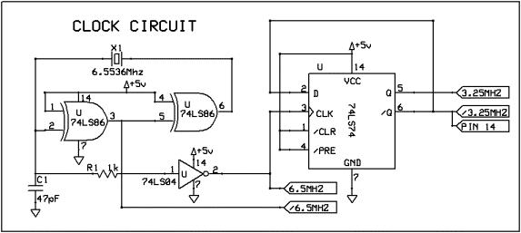
Using the spare gates of the 74ls86 (this is an LS
part) using the design of the zx80 except I use a 6.5536Mhz crystal that is
widely available and less than 1% within the 6.5Mhz that should be used.
Instead of using a third XOR gate I use a simple inverter to give a 6.5Mhz
signal and a /6.5Mhz. This is further divided by 2 to give the 3.25Mhz signal
required by the Z80 CPU it is here that the first mistake can easily be made
you need to connect the /3.25Mhz to ULA pin 14 remember it gets inverted by TR2
on the main board. So that’s 1 pin down 39 to go.
If the VSync pulse is started the OR gate on the left
holds the pair of counters in there reset state (all outputs low) otherwise the
counters will count each of the clock pulses from the 3.25Mhz signal the lower
counter been clocked at 1/16 of the main clock signal when the count reaches
192 the sync becomes active via the 2 input AND gate (connected to Qc an Qd of
the second counter) and will remain so for the next 15 clock pulses until the
count reaches 207 at which point the pair of 3 input and gates in conjunction
with inverters (I didn't have a 7411 which would negate the need for the extra
inverters) almost instantly resets both counters back to zero. So left free
running you get a 15 cycles long pulse every 207 cycles (4.61uS long, every
63.69uS, we are aiming for 4.7uS and 64uS respectively) due to the way the Zeddy
generates the video it is a requirement that the hsync pulses are slightly
short so they remain synchronized with the video from the zeddy. The hsync
pulses are also used for the /NMI pulses if the NMI I turned on.
2. ROMCS and RAMCS control
--------------------------
This is the simplest part of the ULA design.
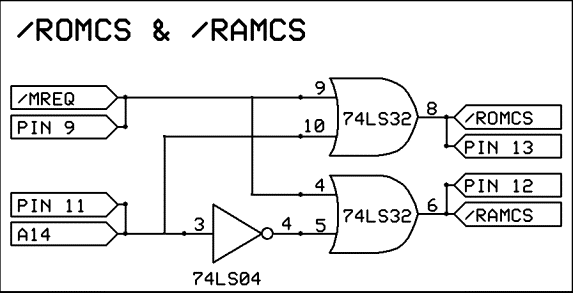
Takes A14 and OR's it with /MREQ to generate the
/ROMCS signal (both A14 and /MREQ low).
Takes an inverted A14 and OR's it with /MREQ to generate
the /RAMCS signal (A14 high and /MREQ low).
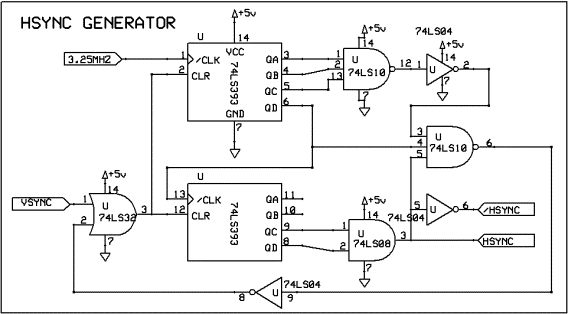
3. VSYCN, NMI and HSYNC control
-------------------------------
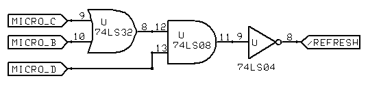
Another circuit that many will be familiar with.
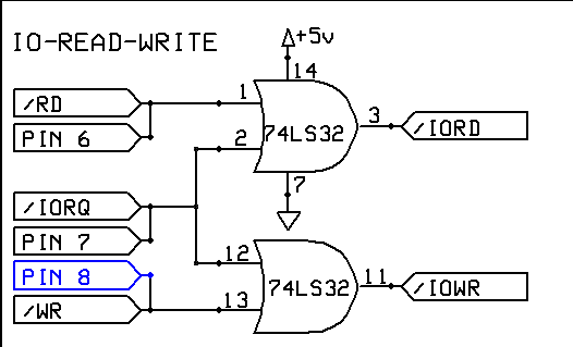
Simple io control circuit, gives a low on /IORD or
/IOWR depending if its a read or write IO instruction used in the next circuit
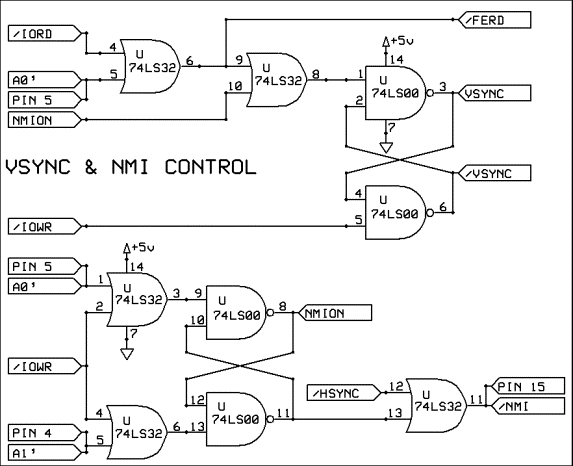
This circuit is quite simple as long as you understand
how a nand gate RS latch works, there are 2 latches used in the zeddies one for
the VSYNC pulse (the top latch) and one for the NMI on or off control the
(bottom latch)
So a read on port $FE [ IN A,($FE) ] will always read
the keyboard and if the NMI generator if off will also toggle the RS latch
starting the VSync pulse and stopping the hsync generator.
Any port write will stop the VSync pulse and restart
the hsync generator.
The NMI control is done of two separate ports, a write
to port $FE will turn on the NMI generator, and a write to port $FD will turn
off the NMI generator.
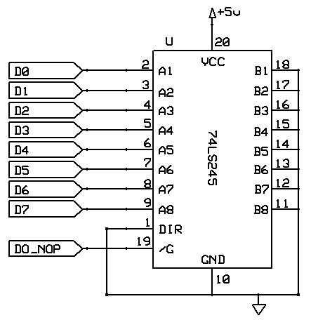
4. keyboard/tape port
---------------------
This is quite simply a 8 bit bus transceiver configured
to always working one direction only bus B to bus A and is enabled via signal
/FERD from the above circuit.
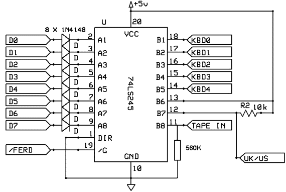
D0 thru D7 connect to ULA pins 32,30,28,26,24,23,21
and 19 respectively.
KDB0 thru KBD4 connect to ULA pins 33,31,29,27 and 25
respectively.
TAPE in connects to ULA pin 20
UK/US connects to ULA pin 22
Uk/us is connected to r30 on the main board in the
absents of r30 a logic high is insured by the 10 resistor connected to B7.
Since as bit 6 is not used it is simply connected to +5v
Tape in during testing it was found that capacitor c10
slowly charges and no signal can be read the tape port becomes unresponsive by
putting a highish value resistor to ground the tape port can be made to work
again, some tweaking of this value may ensue in the weeks to come.
Kbd0 thru kbd4 connects to the 5-way keyboard
connector, no need for pull-ups as they are provided already on the main board
in resistor pack 3.
D0 thru D7 connects via small signal diodes to form a
psuedo open collector output as described earlier this should ensure that
external devices that use port $FE still function correctly.
So that’s all the easy bits done now for the most
complex part of the design and which having had to reproduce its behavior makes
me rather wonder how the boffins at sinclair came up with the idea in the first
place?
Onward we go.
5. The video circuit which itself can be split
----------------------------------------------
a. Character code latch
b. Alternate address generation
c. NOP circuit
d. Shift register
Before I go into each part of the video generation
circuits I needed some way to coordinate the timing of the various actions.
Looking at the timing diagrams for the Z80 CPU during an M1 instruction fetch
cycle we can deduce that /M1 goes low very soon after the rising edge of T1 and
stay so until the shortly after the rising edge of T3 (the start of the
refresh), the data bus is sampled for the instruction fetch on the rising edge
of t3, so to force a NOP to be executed we need to ensure that all lows are
presented on the data bus no later that this. But due to the design of the zx81
we need to read the data bus before hand to obtain the character code used
later to generate the alternative address lines during the refresh, now nearly
every Z80 instructions M1 cycle is 4 t states long, but there are a few that
last longer
LD SP,HL is 6
tstates
PUSH qq is 5
tstates
INC qq is 6
tstates
DEC qq is 6
tstates
DJNZ e is 5
tstates
RET cc is 5
tstates
RST p is 5
tstates
So do we need to take special precaution about these
instructions? Further reading of the Z80 Technical Docs suggest that even on
these instructions with the longer M1 cycles that refresh is still performed
during T3 and T4 so as long as whatever I plan to do does not extend past T4
should be fine. So I originally I was going to create a fake refresh signal
within the ULA design by utilizing the fact that /MREQ goes low but neither /rd
or /wr go low during the refresh, however that was a bit glitchy to say the
least so I came up with another idea
The MICRO COUNTER, is a four bit counter that starts
to count at the beginning of each /M1 cycles and reset to zero on the rising
edge of the 4th t state just in time to start counting again. Using the 6.5Mhz
clock signal as the lowest bit its possible to split the 4 t states into 16
time zones. It was found that I only needed to split it into 8 zones
corresponding to each half cycle of the CPU clock during the M1 cycle. This
counter is used to trigger the various events during the Forced NOP cycle
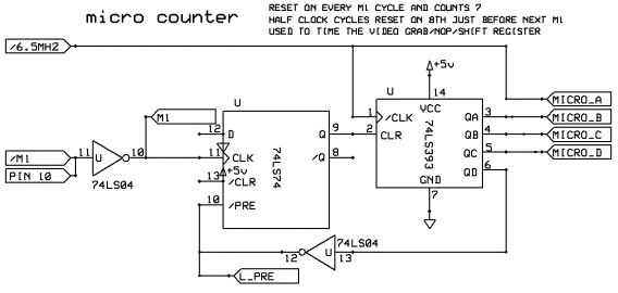
When /M1 goes low the inverter clocks the positive
edge triggered D flip flop which then outputs a low on it Q output this
releases the active high clr input on the counter which is clocked at double
the CPU clock by the /6.5Mhz signal when the count reaches 8 it presets the Q
output via the other inverter, clearing the count back to zero ready to be
triggered again by the next M1 cycle by resetting at 8 it ensures that our
circuit will not interfere with any instruction that has a longer M1 cycle. The
signal L_PRE is used to preset the NOP THIS CYCLE Flip flop at the end of each
cycle.
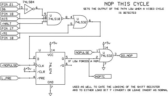
The next Flip flop in the video circuit detects
whether this M1 cycle is a video cycle or not, by using D6, A15, /HALT and /M1.
The latched output will remain in the low state until the rising edge if the
next CPU M1 cycle, it is preset to 1 when my micro counter reaches 8.
This little circuit controlled by the count of the
micro counter determines in conjunction with the above circuit when a NOP
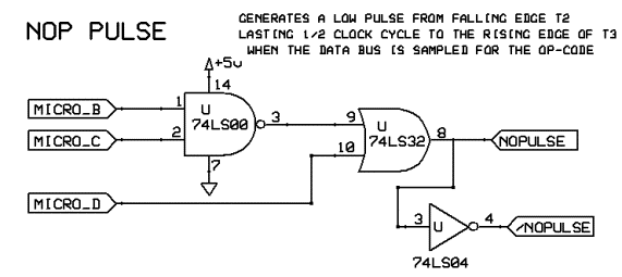
should be forced, when my micro counter reaches 3 at the falling edge of T2 and
holds it until the rising edge of t3 when the CPU samples the data bus for the
op-code. After this my circuit releases the data lines.
Also at the falling edge T2 my circuit grab the data
that was on the data bus immediately before the NOP is forced.
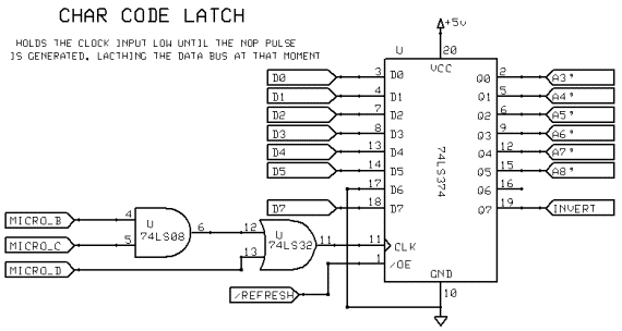
D0 thru D7 connected to ULA pins 32,30,28,26,24,19
This 8 bit latch is controlled by my counter it
latched whatever is present on the D inputs on the rising edge of the CLK
input, The and or logic to the left holds the CLK input low until the falling
edge of T2 when it is driven high and held high until the end of T4. its output
is control by an internal refresh signal. Generated by the following circuit.
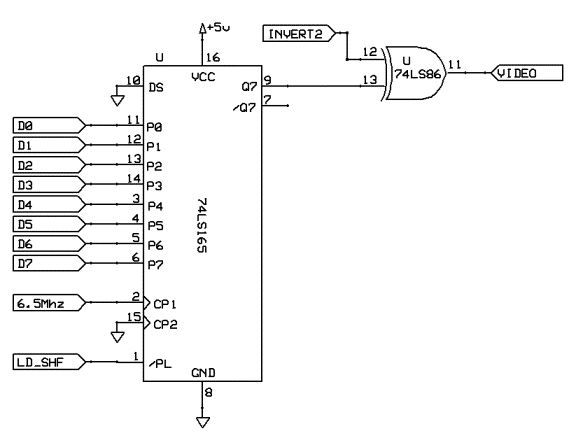
Output Q7 (invert is used in the video invert latch further down the page)
Which enables the output to the alternative address
lines from the falling edge of t3 up until the end of T4. this signal is also
used to enable the line counter output onto alternate address lines A0’ , A1’
and A2’
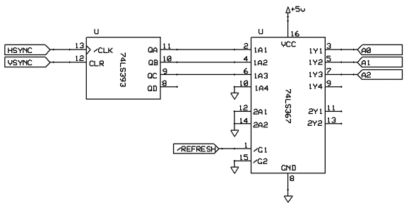
the counter is reset on every VSYNC back to 0 an then
counts every hsync pulse the lower 3 bits of this count are then gates by the
refresh control tristate buffer.
once again D0 thru D7 are connected to ULA pins
32,30,28,26,24,23,27 and 19 respectively. This is the bit that actually forces
all logic lows (B inputs tied to ground) when the outputs ( the A bus) are
enabled the CPU data lines are forced low, forcing the NOP cycle.
That leaves us with the video inverter and shift
register lets take a look at the video inverter first
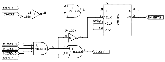
The video inverter circuit consist of a flip flop that
latches the state of the invert bit of the character code from the char code
latch but only if this cycle was is a forced NOP, if it is not a forced NOP
then the top or gate allows the invert bit7 through to the D input ready to be
latched every time when the micro counter reaches 7 falling edge of T4, if it
is a forced NOP cycle also via the bottom or gate the shift register is allowed
to load the new character pattern, otherwise it will continue to load in white
video via its serial input below.
All that remains now is to get the VSync, Hsync and
Video all together to produce a useable composite video signal
This is done with the following.
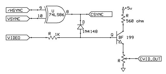
Which combines the Hsync and Sync to give a low output
which turns off Q making the output 0V
Whilst the live video signal drives the emitter
follower to give the final composite video.
And now the moment you have all been dying to get too.
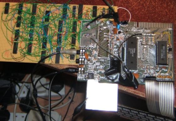
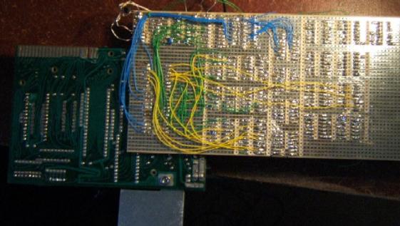
Some real pictures, it’s not pretty and I real ought
to take it apart and rebuild it from the schematics to check there right.
The View from the top.
And from the bottom
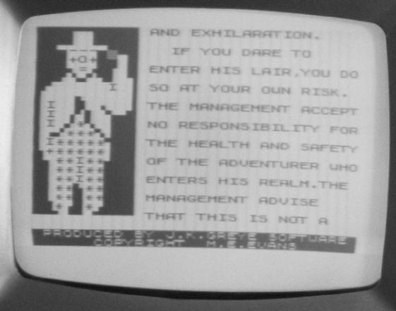
And it would be no good with out TV pictures.
The first full
straight screen I managed to get.

The opening screen from 3d monster maze.
The text based first screen from 25thannni.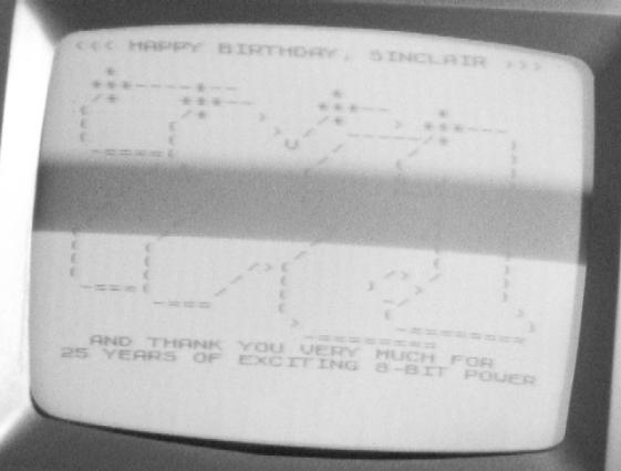
And some hi-res too 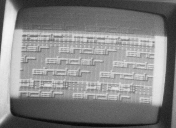
More hi-res 
So That wraps up my finest project so far with the
Zeddy I know that during the writing of this I have seen better and simpler way
of doing things so I may be back with a VERSION_2 ULA replacement.
Regards and best wishes to all Zeddy fans
Andy Rea