![]()
![]()
![]()
![]()
![]()
![]()
![]()
![]()
![]()


All my content and ptohos

Central Processing Units
Why the processors cannot be interesting? Among typical units used in old PCs like Intel 2 or 386, some AMD and clones, there are some interesting chips with not so much known history. This page shows some of these chips.
386 and 486 clones
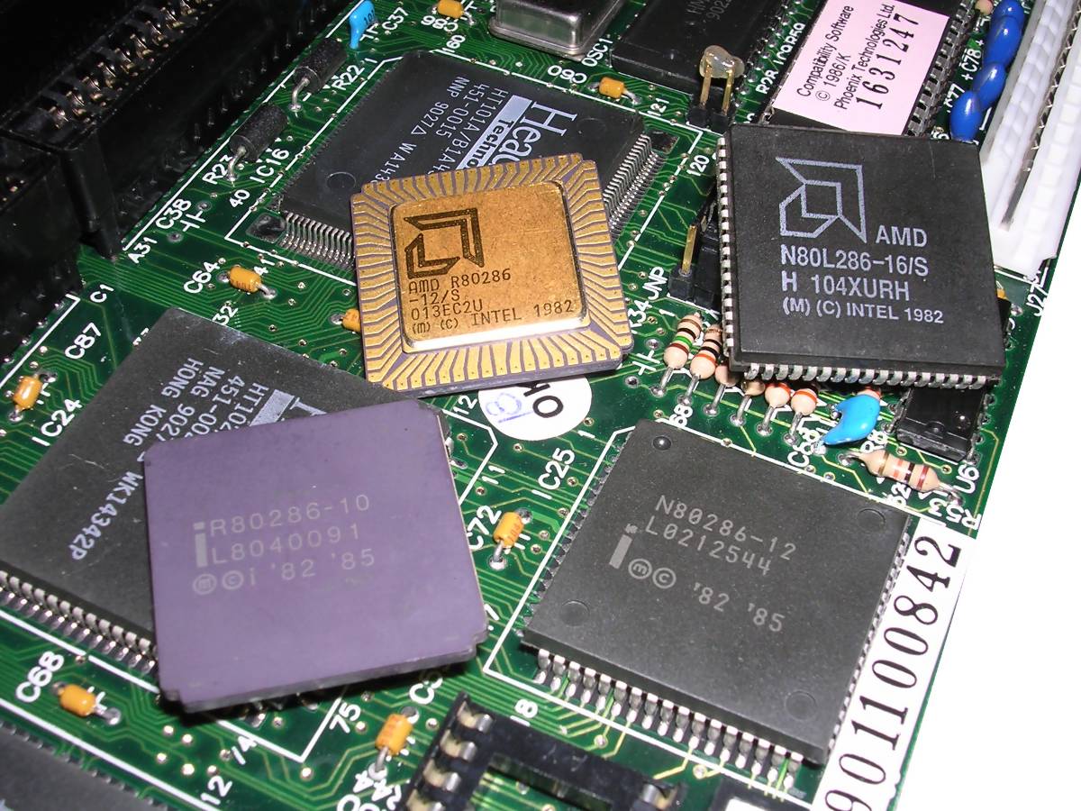
| In first PC times, the development of CPUs was quite equal. Intel manufactured their 8088 and 86, while some other companies made their replacements which were comparable both in functions and speed. A small exception was Nec with their V20 and V30 processors with a bit better instruction set, but not all mainboards could have it and not all programs could use it. With introduction of 286, the situation changed a little - alternatively to Intel, mainboard could contain AMD, Harris or even Fujitsu chip, and sometimes these chips were able to be clocked at higher frequency (Harris 286 could work even at 25MHz!) or were more energy-efficient. On the right you can see different 286 chips in different packages. |
 |
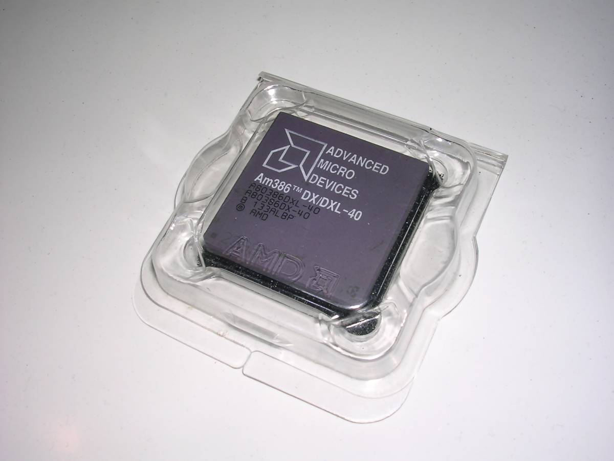
| Introduction of 386 processor changed the situation. While
Intel decided to stop at 33MHz, forcing customers who wanted a
faster processor to choose a 486 series, AMD went to 40MHz,
making it one of the most popular processor in Taiwanese
mainboards. Even some 33MHz Intel mainboards could run 40MHz AMD
with some hardware tweaks. Thus, AMD processors were available
both as a chip to solder into mainboard, a separate piece of
silicon (photo on the right) or, in cheaper version, a soldering
version on a board which converted it to a "socket" processor. When Intel released 486, they allowed some companies to make CPUs on a license, as well as they started to sell licenses for making older chips. In early 1990s they sold a 386SX (a crippled 386) chip license to IBM, then IBM started to make their own chips exclusively for IBM computers - a 386SLC - a 386SX with power management features and on-chip 8kB of cache. These features made the SLC, which was in fact an accelerates 386SX, sometimes faster than Intel's 386DX of the same clock speed. The next CPU, called Blue Lightning, was more engineered to have a complete 32-bit support and was even sometimes called "the fastest 386". |
|
Later, around 1993, when agreement with Intel expired, IBM made another agreement with Cyrix, making a 486-equivalent which was sold as "Blue Lightning" too. They had more in common to Cyrix 486DX2 than to earlier designs made with Intel. Both of these chips, IBM and Cyrix, can be seen in the picture below. The Cyrix chips were not clones of Intel chips, but were re-designed from scratch as functional replacements, so the speed can be a bit different. However, in 1993 Cyrix was accused by Intel for copying the CPU solutions - finally it was dismissed, but caused significant delays for Cyrix.
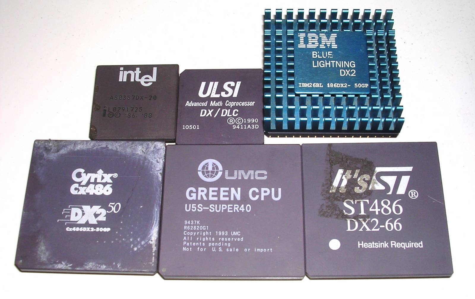 |
Different non-Intel CPUs from 386/486 era, as well as
math coprocessors for 386. From top-left to bottom-right: Bottom row: |
Remember these Cyrix accusations when we'll discuss
another 486 alternative - a small Taiwanese manufacturer re-designed a
486 adding power management features and sold it as Green CPU model
SUPER40 (bottom row, middle in the picture). There were versions
corresponding to SX and DX CPUs, as well as 3.3V chips for e.g.
notebooks or embedded systems, running at 25, 33 or 40MHz. And... Intel
accused them of course, also in 1993, for the same thing as Cyrix.
However, although the patent violations were exactly the same, it ended
a different way - UMCs had to be sold outside USA, and it's clearly
marked in the casing. Why? A typical Kafka's illogical case - Cyrix was
manufacturing their 486s in companies, which previously paid Intel (by
licenses), like ST (the last CPU in the picture) or Texas Instruments,
while UMC did it with their own effort.
Evolution of Pentium form factor
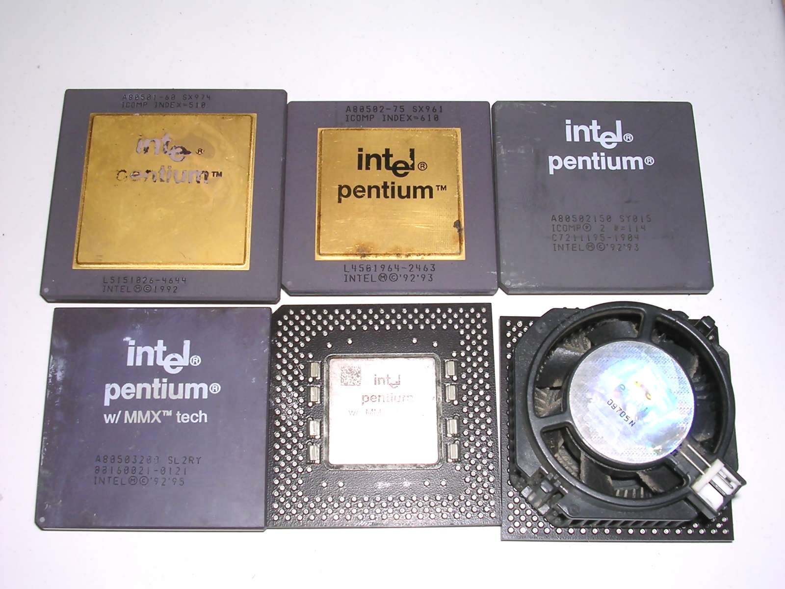 |
Different Pentium processors: Top row: Bottom row: |
The initial Pentium processor with "P5" core, used a 5V
socket designed especially for it. Intel released 60 and 66MHz versions
of Pentium processors for this socket, and switched to Socket 5, in
which 3.3V processors could be used and pins were packed more densely.
Starting from 75MHz, Pentiums were using Socket 5.
With Pentiums becoming more and more complex, Intel decided to add
support for two voltages for one processor. It was introduced around
1995 with Socket 7, which was backwards compatible with Socket 5 CPUs if
mainboard's regulation circuits allowed. It became even more useful
with introduction of Pentium MMX in 1996.
During this development cycle, Pentiums changed their packages. First
ones used only ceramics or had a gold heat spreader (early units). Later
CPUs, without MMX, returned to ceramic packages. With introducing of MMX
technology heat became a bigger problem, so only some units were made of
ceramic - more used plastic packaging with metal heat spreader (in fact
most mobile units) or had a
special package with heatsink built-in, plastic or ceramic.
Interesting thing is a Pentium 300MHz, probably a fake one (overclocked
266MHz), can be seen
in this collection.
Although Intel kept their Pentium architecture in secret, there were alternatives. AMD released their K5 chips in 1996, which was a re-design closer to Pentium Pro. The idea was to use some fast RISC core and command translation logic, which was different than Pentium's approach. So because Pentium and K5 of the same clock had significantly different computational speed, AMD introduced a measure called PR - Performance Rating or "Pentium Rating". The chip with PR166 was working more-or-less as quick as Pentium 166MHz, regardless of its "real" frequency.
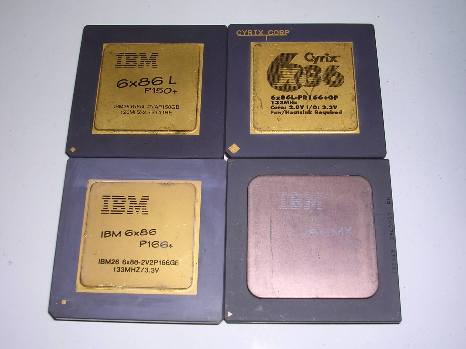 |
IBM Pentium replacements: Top row: 1 - IBM 6x86 120MHz (PR150) 2 - Cyrix 6x86 133MHz (PR166) Bottom row: As it was noted in part 1, we left IBM with contract with Cyrix for making their CPUs. As Pentiums became more and more popular, Cyrix had their own Pentium-equivalent called 6x86 and they manufactured it also using IBM's plants. The 6x86 was in fact a deeply re-designed Pentium, so there was no code translation like in AMD's K5. Additionally, early units had compatibility and heat problems, so Cyrix put a "Heatsink/Fan required" text on their processors. |
The speed in integer benchmarks was indeed slightly
outperforming Pentiums. However, the engineers focused more on the
branch prediction and I/O optimizations than on floating point unit
which was much slower than Pentium's, comparable to Cyrix 486s (maybe
they used just the same circuits?). They somewhat partially got out of
problem marketing 6x86 CPUs as... processors for office applications,
where math co-processor is used more rarely than in e.g. multimedia or
CAD.
A tip of the moment: Quake shows reasonably well and smooth on 100MHz
Pentiums. In 133MHz Cyrix frames are lots all time.
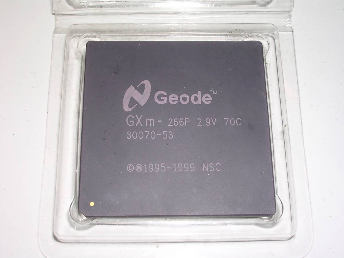
| In the picture on the right we can see an interesting
processor: The Geode, made by National Semiconductor in
mid-1990s. Although this chip can physically fit into Socket 7,
it is not compatible on a software level. Why? Because there is
almost a complete computer inside. There is a Cyrix MediaGX-like core with MMX, 12kB of cache, memory interface, PCI controller, and a CS5530 module which is a video and sound chip. Most typical chipset functions are implemented in this CPU, so it needs a special mainboard and chipset. Being designed for embedded systems, Geode is also a low-power chip. The only problem is that many of these features directly decrease the computational speed. 300MHz Geode is comparable to Pentium running at 200-233MHz. This chip is a 266MHz. The Geodes found their place in embedded/control systems, thin clients or point-of-sale terminals. They were also used in some notebooks being frequently reported as "CyrixInstead" CPU (its ID). The Geode line was made by Cyrix, then National Semiconductor, finally being taken by AMD in 2002. |
 |
Pentium II and III, and Slot 1
| Slot 1 was an attempt made by Intel to make own
CPU connector exclusively for own CPUs and introduce new
features. Slot 1 is a slot for circuit board, in which CPU is
soldered in, as well as cache chips. Simulatneously AMD
introduced similar slot - Slot A. Slot CPUs could be used in
SMP, so it was possible to use 2 CPUs in special mainboards. For
a really high-end server purposes, a Slot 2 was used, an
extended Slot which was targeted towards multi-processor
systems.
Unfortunately, there were significant problems with these
Slots. First of all, production was problematic - if a typical
single single CPU failt factory tests, a CPU is discarded. If a
Slot 1 CPU fails, a whole module is discarded - with cache chips
which are good and cannot be re-used. Similarly if cache chips
fail, a good CPU is discarded. |
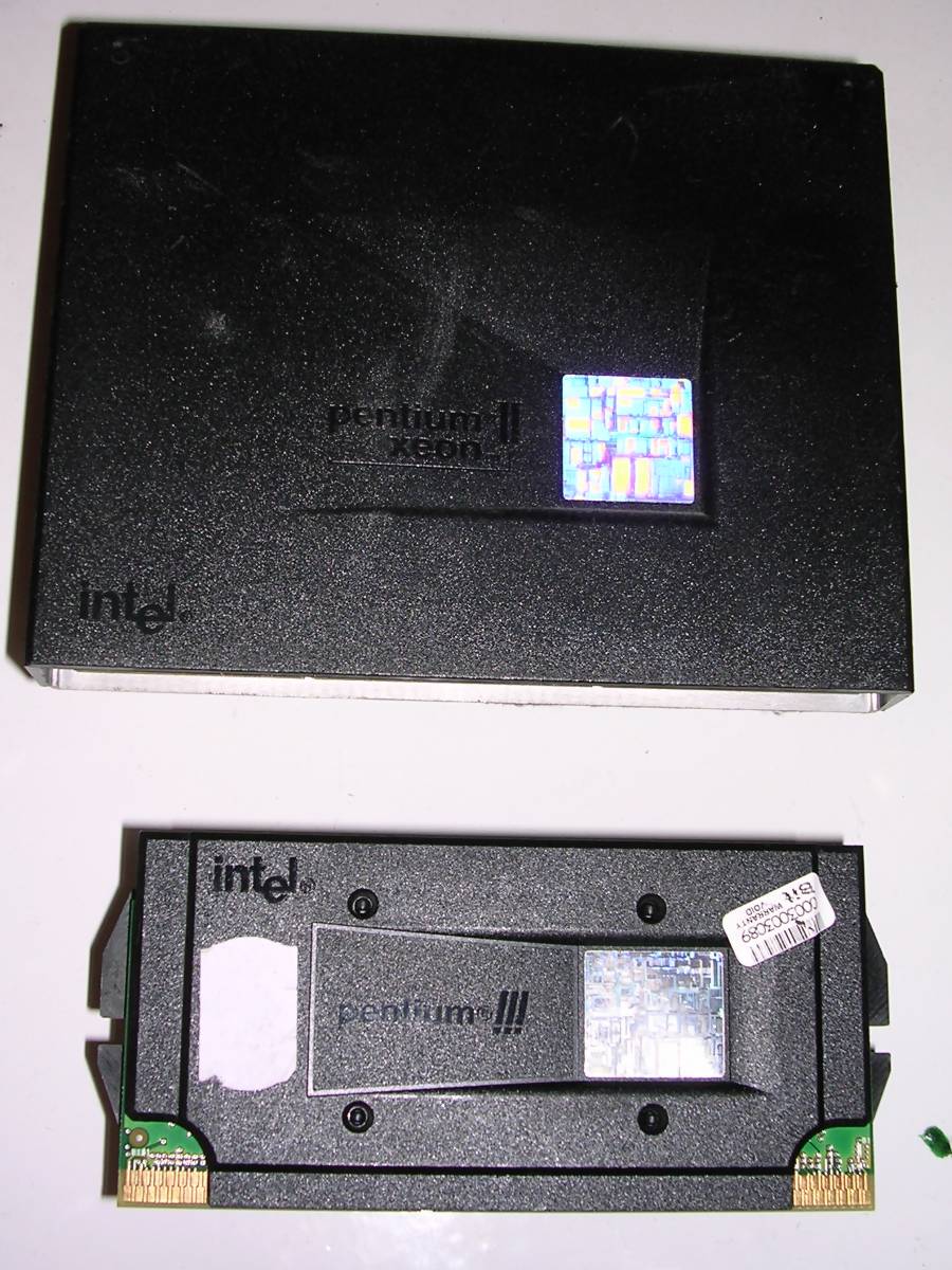 A
Slot 2 Pentium II Xeon (upper) and Slot 1 Pentium III (lower) A
Slot 2 Pentium II Xeon (upper) and Slot 1 Pentium III (lower) |
||
| One of the highest frequency CPU for Slot 1 was Pentium III at 866MHz. In many mainboards uncertain connections caused it to be unstable even at 800MHz. | |||
|
|||
http://www.cpu-world.com/ - CPU
World - the biggest source of information about old and new processors
in the Internet.
http://www.cpu-collection.de/
- Collection of various CPUs