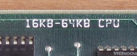
Parent

IBM 5150:  RAM on a '16KB - 64KB' Type of Motherboard


5150_label_16kb_64kb_cpu.jpg


4 banks of 16 KB motherboard RAM, providing up to 64 KB of conventional memory.

RAM chips of type 4116 are used, of an access time rating of 250 ns (or faster, e.g.  200 ns).  4116 examples.
250 ns is the figure that appears in IBM's technical reference for the 5150.

Bank 0: 16 KB sized,  addressed 0000 to 3FFF hex  (  0 KB to 16 KB)   (soldered to motherboard)
Bank 1: 16 KB sized,  addressed 4000 to 7FFF hex  (16 KB to 32 KB)   (socketed)
Bank 2: 16 KB sized,  addressed 8000 to BFFF hex  (32 KB to 48 KB)   (socketed)
Bank 3: 16 KB sized,  addressed C000 to FFFF hex  (48 KB to 64 KB)   (socketed)

Click here for a diagram that shows the bank and bit layout on the 5150 motherboard.


Increasing conventional memory

Additional conventional memory can be provided by way of expansion cards, however, in an IBM 5150, all four banks of motherboard RAM must be populated before RAM can be added by way of expansion cards (source: Note on page 5-34 of the APR84 edition of the Guide To Operations manual).  That is because, on a 5150 motherboard, all four banks are permanently enabled.  Click here to see an example.

Note that BIOS supplied with the 16KB-64KB motherboard only recognises up to 544 KB of RAM.  This limitation is purely because, by design, the BIOS only reads the first 4 switches in switch block SW2.  Consider that in 1981, even 128K was considered to be a lot of RAM for a personal computer.  This limitation can be removed by upgrading the BIOS to the 10/27/82 one.


RAM related switch settings on motherboard

SW1

Switches 3 and 4 on switch block SW1 are set according to how many banks of RAM are populated on the motherboard (however, if you have the 10/27/82 BIOS, note the bug described in the following section).
On a 5150 motherboard, those two switches do not enable/disable the motherboard's banks of RAM; instead, used to inform the BIOS of bank population.
Click here for SW1 settings.

SW2

The switches on switch block SW2 are set to the total amount of conventional memory fitted in the 5150 (that is, on motherboard + on expansion cards).
If you set SW2 to a LOWER amount than is fitted, there is no error - the motherboard will only recognise what was set per SW2.
If you set SW2 to a HIGHER amount than is fitted, there is a 201 memory error.

Click here for SW2 settings.


RAM implications of upgrading the BIOS to the 10/27/82 one

As supplied from the factory, this motherboard was only fitted with either one of the following two BIOS revisions:
1.  Dated 04/24/81.  Chip U33 has "5700051" printed on it.
2.  Dated 10/19/81.  Chip U33 has "5700671" printed on it.

Later, IBM provided a BIOS upgrade kit for this motherboard, making the BIOS the same revision (10/27/82, "1501476" printed on U33) as found on the 64KB-256KB motherboards.
The new BIOS recognises up to 640 KB of RAM (and recognises BIOS expansion ROM's).

There are two important RAM implications of using the 10/27/82 BIOS in a 16KB-64KB motherboard:
1.  Different switch settings apply to SW2: Switch number 5 in switch block SW2 is now used.  Click here to see an example.
2.  Due to a bug, the 10/27/82 BIOS will almost always generate a 201 type error (e.g.  "1094 201") if you do not populate all 4 banks of motherboard RAM.  If desired, click here for technical details about the bug.


POST test of conventional memory

During the 5150's Power-On Self Test (POST), the POST tests the conventional memory that is specified by the setting of the SW2 switch block.

If a problem is found in the first 16 KB, the POST will halt.  It will appear to you that the motherboard is 'dead'.  For further information, see the section below titled 'Failure of first 16 KB'.

If a problem is found in the remaining RAM, a 201 type error is reported on-screen.  The format of a 201 error produced by a 5150 is "aabb 201".  An example is "0510 201".
The "aa" portion of "aabb" indicates which 4 KB address block contains the address at fault.
The "bb" portion of "aabb" indicates which bit/s in the block is/are faulty.

You can use the diagram here to calculate the failing address block and bit/s, but also read the 'Multiple bit failure' section below.


Address Block Indicator

The following table is specific to the 16KB-64KB motherboard.

Value of 'aa' in 201 error Corresponds to RAM bank Address range of bank            Comment
00 to 03 Motherboard bank 0 00000 to 03FFF hex   (  0 KB to 16 KB)  You will never see this.  See 'Failure of first 16 KB' section below
04 to 07 Motherboard bank 1 04000 to 07FFF hex   (16 KB to 32 KB)   
08 to 0B Motherboard bank 2 08000 to 0BFFF hex   (32 KB to 48 KB)   
0C to 0F Motherboard bank 3 0C000 to 0FFFF hex   (48 KB to 64 KB)   
10 to 9F RAM on an expansion card/s 10000 to 9FFFF‬ hex   (64 KB to 640 KB) Cannot elaborate - too many different types of RAM cards

Click here for a diagram that shows which banks are where on the 5150 motherboard.


Bit Indicator

Value of 'bb'
in 201 error
Bit at fault            Comment
00 parity  
01 bit 0  
02 bit 1  
04 bit 2  
08 bit 3  
10 bit 4  
20 bit 5  
40 bit 6  
80 bit 7  
other [multiple] Multiple bits.  Use the diagram here to calculate the failing bits, but also read the 'Multiple bit failure' section below.

Click here for a diagram that shows which bits are where on the 5150 motherboard.


Multiple bit failure

If multiple bits are indicated, note that sometimes that is because non-existent RAM is being tested by the POST.  For example, if I remove the RAM expansion card from my 16KB-64KB motherboard (without doing anything else), then I see the start-up error of "1098 201", a bit indicator of 98.

Example causes of non-existent RAM being tested:
* SW2 set for more RAM than is actually fitted to the 5150
* An expansion card that provides RAM is faulty
* An expansion card that provides RAM is incorrectly configured


Failure of first 16 KB

The first 16 KB corresponds to bank 0, the soldered-in bank.  That bank (like the other three) cannot be disabled.

The Power on Self Test (POST) component of all three possible BIOS revisions check the first 16 KB, bank 0, at power-on of the 16KB-64KB motherboard.  If the POST discovers that any of the chips in that bank are faulty, the POST will stop, providing no indication whatsoever (visual or audible).  To you, it will appear that the motherboard is 'dead'.

One way to diagnose this particular problem is to use a suitable SuperSoft/Landmark diagnostic ROM in socket U33 (replacing the existing BIOS ROM).

The piggybacking technique will sometimes diagnose this particular problem.


4116 RAM chip

This chip requires 3 power sources: +12V, -5V, +5V   (diagram)

Therefore, if you have what appears to be a 'dead' 16KB-64KB motherboard, then one of the things to check is that the power supply is producing the fore mentioned three voltages.