| Parent |
| Motherboard | Expansion card | Information source | |
|---|---|---|---|
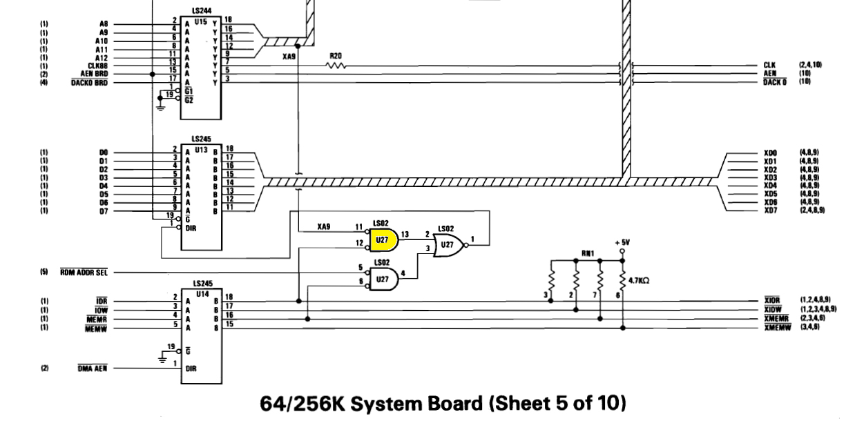
| 5150 | 000 - 1FF hex | 200 - 3FF hex | Reference: The IBM 5150 document here 1. Page 1-41: Read gating circuit (part of chip U27) for motherboard I/O, looks for A9 being low (0111111111 = 1FF). See here. 2. |
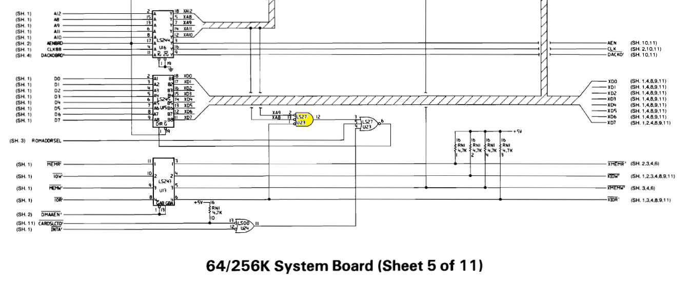
| 5160 | 000 - 0FF hex | 100 - 3FF hex | Reference: The IBM 5160 document here 1. Page 1-39: Read gating circuit (part of chip U23) for motherboard I/O, looks for both A8 and A9 being low (0011111111 = FF). See here. 2. Page 1-24 |