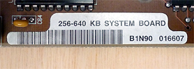
Parent

IBM 5160:  RAM on a '256 - 640KB' Type of Motherboard


5160_label_256_640kb.jpg


Motherboard RAM consists of two banks of 256 KB (in banks 0 and 1), plus two banks of 64 KB (in banks 2 and 3), providing up to 640 KB of conventional memory.

The two banks of 256 KB use RAM chips of type 41256, of an access time rating of 200 ns (or faster).  41256 examples.
The two banks of 64 KB use RAM chips of type 4164, of an access time rating of 200 ns (or faster), and of the type where pin 1 is not used (Not Connected).  4164 examples.

200 ns is the figure that appears in IBM's technical reference for the 5160.

Bank 0: 256 KB sized,  addressed 00000 to 0FFFF hex  (    0 KB to 256 KB)   (socketed)
Bank 1: 256 KB sized,  addressed 40000 to 7FFFF hex  (256 KB to 512 KB)   (socketed)
Bank 2: 64 KB sized,  addressed 80000 to 907FF hex  (512 KB to 578 KB)   (socketed)
Bank 3: 64 KB sized,  addressed 90800 to ‭9FFFF‬ hex  (578 KB to 640 KB)   (socketed)

Click here for a diagram that shows the bank and bit layout on the 5160 motherboard.


RAM related switch settings on motherboard

On IBM 5160 motherboards, switches 3 and 4 on switch block SW1 selectively disable/enable the RAM banks.
The settings are at here.


Increasing conventional memory

The full 640K of conventional memory can be fitted to the motherboard.

However, the IBM 5160 gives you the option of adding conventional memory via an expansion card (one or more) without having to first populate all of the motherboard RAM banks.  An example is shown here.


Design flaw

Be aware of a design flaw, one that affects the 5160's ability to determine how much conventional memory is fitted (on motherboard + on expansion cards).
The flaw is discussed at here.


POST test of conventional memory

During the 5160's Power-On Self Test (POST), the POST tests the conventional memory (the amount that it thinks is fitted).

If a problem is found in the first 64 KB (assumption: 01/10/86 BIOS), the POST will halt.  It will appear to you that the motherboard is 'dead'.  For further information, see the section below titled 'Failure of first 64 KB'.

If a problem is found in the remaining RAM, a 201 type error is reported on-screen.  The format of a 201 error produced by a 5160 is "aaaaa bb 201".  An example is "20000 80 201".
The "aaaaa" portion indicates which address the fault is at.
The "bb" portion indicates which bit/s is/are faulty.

Note however, that because of the design flaw discussed at here, you will not always see a 201 error if a RAM chip has failed (instead, seeing less RAM than fitted).

For a 201 error, you can use the diagram here to calculate the failing bit/s, and the address as a KB figure.

Click here for a diagram that shows the bank and bit layout on the 5160 motherboard.


Failure of first 64 KB

If the POST (assumption: POST in 01/10/86 BIOS) discovers a problem in any of the first 64 KB of RAM, the POST will stop, providing no indication whatsoever (visual or audible).  To you, it will appear that the motherboard is 'dead'.

Note that the first 64 KB corresponds to the first quarter of each chip in bank 0 (256 KB sized).  RAM chips fail in different ways.  Therefore, if a RAM chip in bank 0 fails completely, you'll see the 'dead' motherboard symptom described earlier.  But if a RAM chip in bank 0 fails in such a way that the failure only affects an address/addresses in the last three quarters of the chip, then the BIOS will display a corresponding 201 error.