| 1. |
User turns on power supply. |
| |
|
| 2. |
Motherboard receives +5 volts from the power supply. |
| |
|
| 3. |
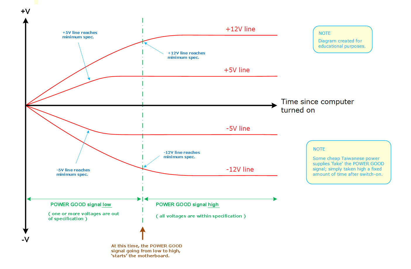
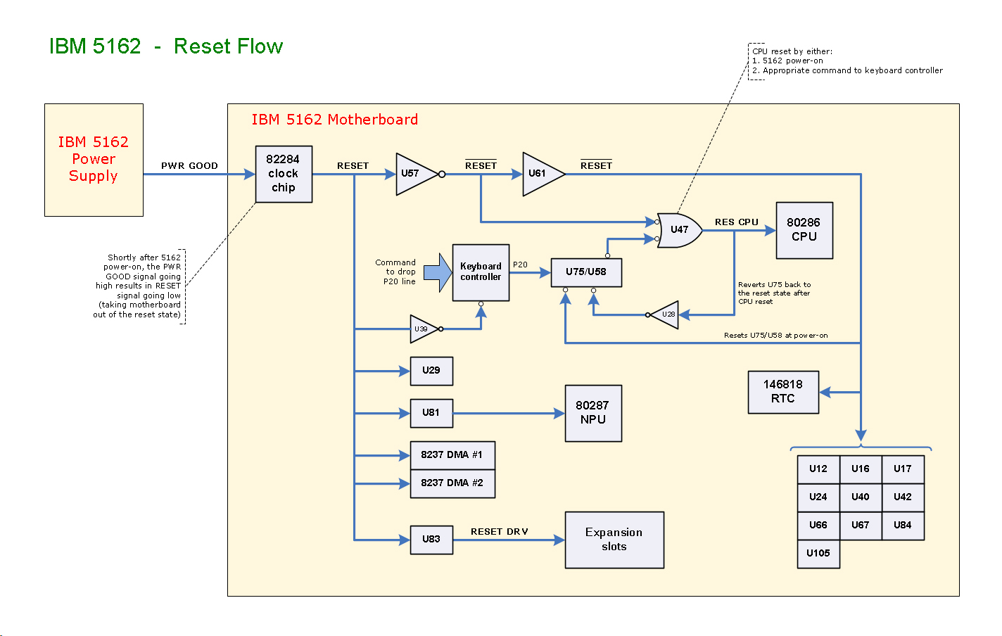
Also received from the power supply is the POWER GOOD signal, a digital signal of TTL levels, which at this time, is low. <----- Important: At this time, the signal is LOW |
| |
|
| 4. |
Because the POWER GOOD signal is low, the motherboard's 82284 chip takes the motherboard's RESET line high. Per here, various chips on the motherboard (including the 80286 CPU) are held in a reset state. |
| |
|
| 5. |
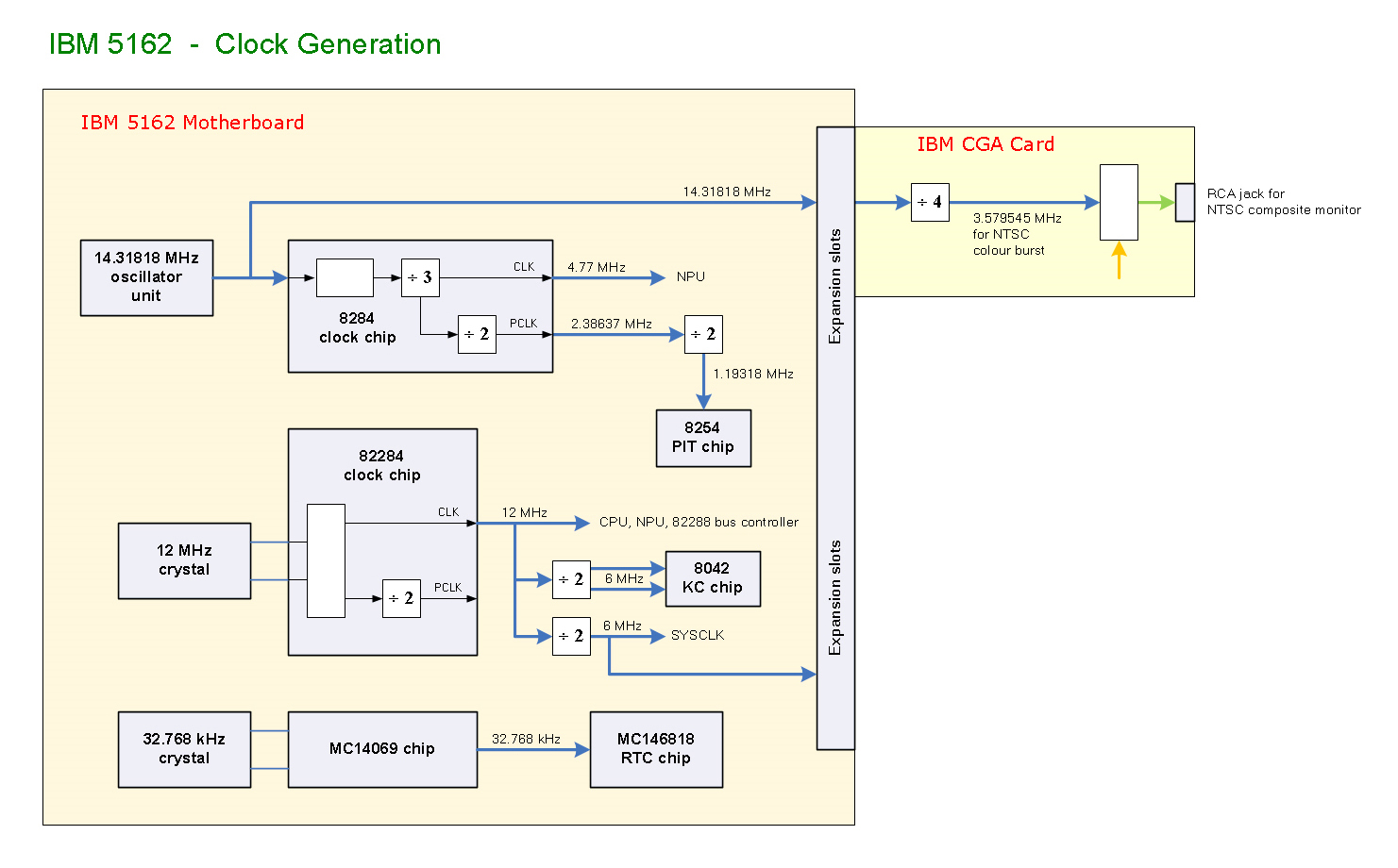
Refer to here. On the motherboard, the 82284 chip generates a 12 MHz clock signal for the 80286 CPU and the 82288 bus controller chip. (And optional 80287 NPU, if fitted.) |
| |
|
| 6. |
Later, when all voltages from the power supply are within specification, the power supply takes the POWER GOOD line high. |
| |
|
| 7. |
When the 82284 chip sees the power supply's POWER GOOD signal go high, it takes the motherboard's RESET line from high to low. As a result, chips are taken out of the reset state. |
| |
|
| 8. |
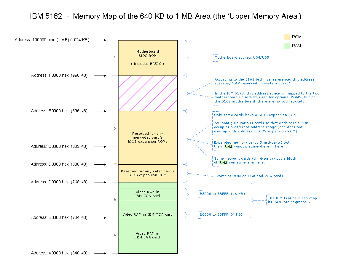
When the 80286 CPU leaves the reset state (see note 1 below), it starts execution at address FFFF0. In the IBM 5162, that address corresponds to an address in the motherboard's BIOS ROM set (per here). |
| |
|
| 9. |
Starting at address FFFF0 are five bytes, which together form a jump instruction to the start of the BIOS' power-on self test (POST). |
| |
|
| 10. |
The POST executes. |
| |
|
| |
If a POST card is fitted, various POST codes will be sent to the POST card as the POST progresses.
|