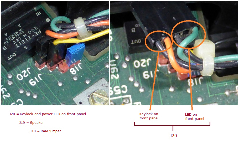
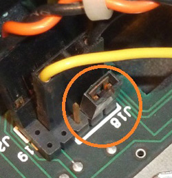
to the power connectors.
Pictured in the rear position (towards rear of computer).
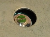
| Home |
|
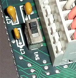
The switch is located adjacent to the power connectors. Pictured in the rear position (towards rear of computer). |
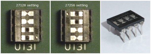
 |
The jumper block is located at the front of the motherboard. Jumper pictured in the '512 KB' position. |