| Home |
| 01/10/84 BIOS | 06/10/85 BIOS | 11/15/85 BIOS | Comment | |
|---|---|---|---|---|
| 01 | 1. 80286 register test 2. Ensure CMOS clock interrupts are disabled 3. Reset video |
1. 80286 register test 2. Ensure CMOS clock interrupts are disabled 3. Reset video |
1. 80286 register test 2. Ensure CMOS clock interrupts are disabled 3. Reset video |
|
| 02 | Verify shutdown byte in 146818 RTC chip | Verify checksum of BIOS ROM's | Verify checksum of BIOS ROM's | For 01/10/84 BIOS, see note 6 |
| 03 | Verify checksum of BIOS ROM's | Verify shutdown byte in 146818 RTC chip | Verify shutdown byte in 146818 RTC chip | Shutdown status byte |
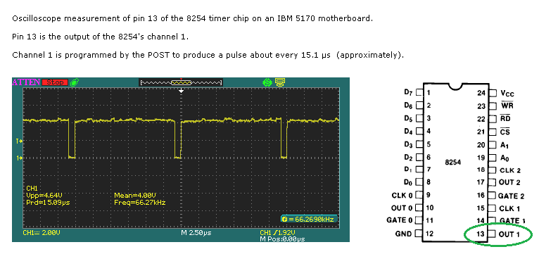
| 04 | 8254 PIT channel 1 - 'all bits on' test | 8254 PIT channel 1 - 'all bits on' test | 8254 PIT channel 1 - 'all bits on' test | Channel 1 of the 8254 timer chip's 3 channels (0/1/2) |
| 05 | 8254 PIT channel 1 - 'all bits off' test | 8254 PIT channel 1 - 'all bits off' test | 8254 PIT channel 1 - 'all bits off' test | |
| 06 | 8237 DMA #1 - initialization and test | 8237 DMA #1 - initialization and test | 8237 DMA #1 - initialization and test | The first of the two DMA chips (the one in socket U111) |
| 07 | 1. 8237 DMA #2 - initialization and test 2. 8254 PIT channel 1 - initialization |
1. 8237 DMA #2 - initialization and test 2. 8254 PIT channel 1 - initialization |
1. 8237 DMA #2 - initialization and test 2. 8254 PIT channel 1 - initialization |
See note 7 for info on channel 1 initialization |
| 08 | DMA page register test | DMA page register test | DMA page register test | |
| 09 | Refresh bit | Refresh bit | Refresh bit | Verify that 'refresh bit' is toggling. See note 9. |
| 0A | 8042/8742 keybd controller - Buffers | 8042/8742 keybd controller - Buffers | 8042/8742 keybd controller - Buffers | See note 8 |
| 0B | 8042/8742 keybd controller - Self test | 8042/8742 keybd controller - Self test | 8042/8742 keybd controller - Self test | Issue a 'self test' command to the keyboard controller |
| 0C | " " " " " " | " " " " " " | " " " " " " | |
| 0D | 8042/8742 - additional tests | 8042/8742 - additional tests | 8042/8742 - additional tests | |
| 0E | If a warm boot, zero first 64K of base memory | If a warm boot, zero first 64K of base memory | If a warm boot, zero first 64K of base memory | No verification done |
| 0F/DD | Test first 64K of base memory | Test first 64K of base memory | Test first 64K of base memory | On failure: 1. If MDA or CGA card fitted, display a 201 error that points to address 000000 2. In a loop, continuously output the POST code of DD (see here) |
| 10 | ||||
| 11 | Verify that PE/MP/EM/TS bits of CPU are zero | Verify that PE/MP/EM/TS bits of CPU are zero | Verify that PE/MP/EM/TS bits of CPU are zero | |
| " | Speed test | Speed test | See note 1 | |
| 12 | 1. 80286 - additional tests 2. Initialise 8259 PIC #1 |
1. 80286 - additional tests 2. Initialise 8259 PIC #1 |
1. 80286 - additional tests 2. Initialise 8259 PIC #1 |
|
| 13 | Initialise 8259 PIC #2 | Initialise 8259 PIC #2 | Initialise 8259 PIC #2 | |
| 14 | Set up temporary interrupt vectors | Set up temporary interrupt vectors | Set up temporary interrupt vectors | |
| 15 | Set BIOS call interrupt vectors | Set BIOS call interrupt vectors | Set BIOS call interrupt vectors | |
| 16 / 17 | 1. 146818 RTC chip - ask if battery is low 2. 146818 RTC chip - verify checksum |
1. 146818 RTC chip - ask if battery is low 2. 146818 RTC chip - verify checksum |
1. 146818 RTC chip - ask if battery is low 2. 146818 RTC chip - verify checksum |
* POST code 17 is only output if battery is low * Checksum of a certain portion of the RAM within the 146818 |
| 18 | Disable parity checking of RAM | Disable parity checking of RAM | Disable parity checking of RAM | Preparation for later |
| 19 | Put 80286 into protected mode | Put 80286 into protected mode | Put 80286 into protected mode | |
| 1A | Verify that 80286 in protected mode | Verify that 80286 in protected mode | Verify that 80286 in protected mode | |
| 1B | Determine size of base memory | Determine size of base memory | Determine size of base memory | See note 2 |
| 1C | Set/reset the 512/640K RAM flag | Set/reset the 512/640K RAM flag | Set/reset the 512/640K RAM flag | |
| 1D | Determine size of extended memory | Determine size of extended memory | Determine size of extended memory | See note 3 |
| 1E | Store extended memory size | Store extended memory size | Store extended memory size | See note 4 |
| 1F | Test address lines 19 to 23 | Test address lines 19 to 23 | Test address lines 19 to 23 | |
| 20 | Exit from protected mode | Exit from protected mode | Exit from protected mode | |
| 21 | Initialise any MDA/CGA video card | Initialise any MDA/CGA video card | Initialise any MDA/CGA video card | |
| 22 | MDA/CGA - Video line test | MDA/CGA - Video line test | MDA/CGA - Video line test | |
| 23 | Process any 'advanced' video card | Process any 'advanced' video card | Process any 'advanced' video card | See note 5 |
| ... | ... | ... | ... | |
| ... | ... | ... | ... | |
| ... | ... | ... | ... |
| DD | See 'OF/DD' above | See 'OF/DD' above | See 'OF/DD' above |
|---|
| Note 1 | Verify that motherboard 'speed' is within certain bounds. Added by IBM to stop the overclocking (via a replacement crystal) that owners sometimes did to early 5170's. On failure, before halting the CPU, the POST also beeps the speaker: 1 long beep followed by 1 short beep |
| Note 2 | Sizing only. First 64K of base memory was tested at checkpoint 0F. Remainder of base memory gets tested at checkpoint 2F. |
| Note 3 | Executed in protected mode. Sizing only. Extended memory gets tested at checkpoint 2F. |
| Note 4 | Stored in the MC146818 RTC chip |
| Note 5 | Video cards that contain a BIOS ROM. The EGA card is an example. The ROM is executed (i.e. card initialises itself). |
| Note 6 | Failure of the 'Verify shutdown byte' has been observed when both of the following are true: * 5170 motherboard has the 01/10/84 BIOS; and * 5170 motherboard inadvertently powered using an XT-class power supply, rather an an AT-class one. |
| Note 7 | Initialise channel #1 of 8254 timer chip, setting a divisor of 18. That results in one output pulse per approx. 15 µs. See here. |
| Note 8 | 1. If output buffer full, flush it. 2. If input buffer full, and 100 ms later is still full, halt the CPU. |
| Note 9 | Verify that channel 1 of the 8254 timer chip is periodically generating a 'RAM refresh request'. So what is being looked at is simply something that triggers a RAM refresh cycle. That is not the same as verifying that RAM refreshing is actually occuring. |