FIC 486-VIP-IO2 Motherboard - Part 1
28th April 2021
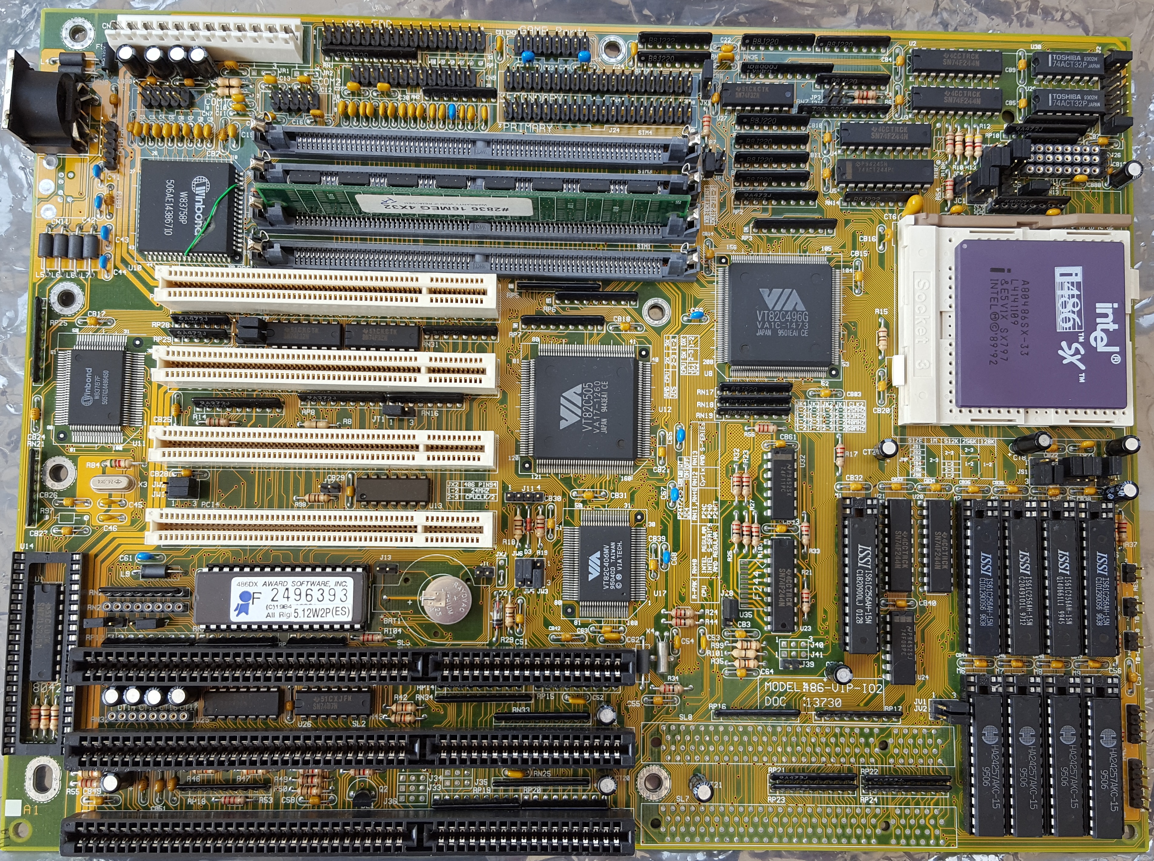
I have owned this First International Computer (FIC) 486-VIP-IO2 board for a good 7 years or so. In fact I bought three of them as a bundle - it cost me £40 delivered. They are all identical, and I got the seller to also throw in three voltage regulators that usually come with these boards and which allow the running of sub-5V CPUs. Here's a quick look at the board:
All three of these boards were identical when I got them, coming with only 128 KB of L2 cache (I upgraded one of them to 256 KB as you can see in the picture above), no CPU or memory, and all had the little wiring fix on the Winbond W83758P "Super I/O" controller chip which is believed to be a factory fix (it was not uncommon for circuit boards to receive a remedial fix if they realised during testing that either the design was flawed or the manufacturing process had failed in some way).
Quick Visual Inspection
Looking around the board it appears to comprise the following:
- A Socket 3 168-pin CPU socket.
- VIA VT82C496G/VT82C505 "Pluto" chipset.
- Award 486DX BIOS v5.12W2P (ES).
- Four 72-pin SIMM slots.
- Two banks of L2 cache slots, both now populated with 128 KB each.
- Three 16-bit ISA expansion slots, four PCI slots, and solder pads for two VLB slots.
- AT P8/P9 power connector
- Full-size DIN keyboard socket
Date-wise, the most recent date stamp on the motherboards' chips is week 04 of 1995, which is the tiny VIA chip. So this board was manufactured after 1st February 1995.
The Component Parts
The CPU Socket
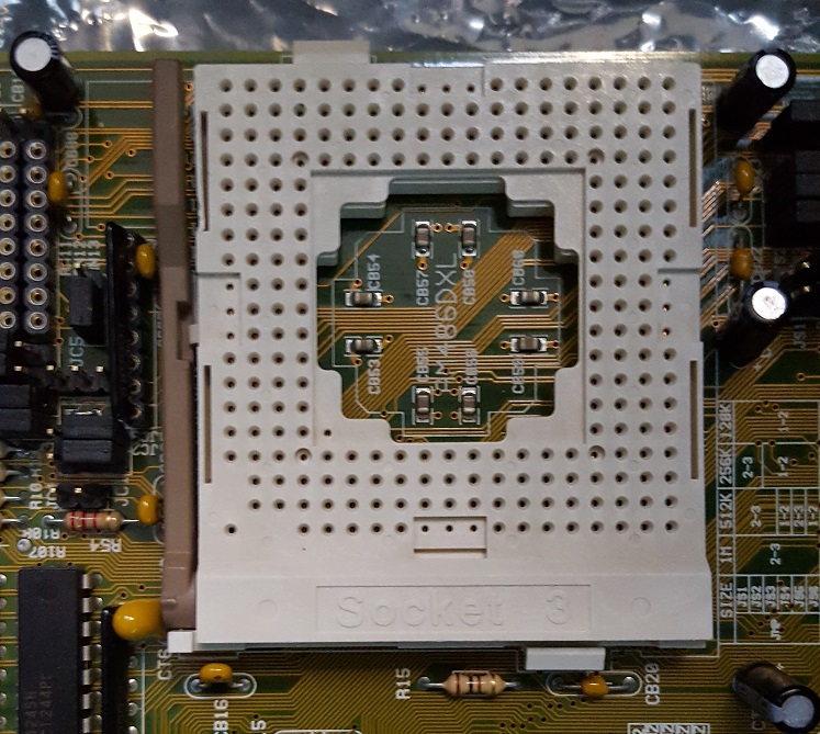 Being a Socket 3 motherboard puts it firmly in the 486-era. Given that the board has a voltage regulator accessory allowing it to drive CPUs ranging from 3.3V up to 5V, this board actually has a very good level of CPU compatibility - here is the list of supported CPUs:
From Intel: 80486SX, DX, DX2, DX4, Pentium OverDrive , plus S-series variants of these processors.
From AMD: Am486DX, DX2, DXL2, DX4, and DXL4.
From Cyrix (and other-branded equivalents from TI, IBM, and SGS): Cx486S (FasCache), and Cx486DX.
All of the above can be made to run from 25 MHz up to 100 MHz, making it a useful motherboard to be installed in a retro PC if targeting 1989 to 1995 era.
The Chipset
The motherboard uses the VIA "Pluto" chipset, launched in late 1994, so it pre-dates the famous "Apollo" chipsets that served on the Socket 7 platform, but is a late-486 chipset. This two-chip chipset consisted of:
- VT82C496G - CPU, Cache, Memory, ISA/PCI/VLB Bus Controller and Keyboard controller
- VT82C505 - VLB to PCI Bridge
The chipset's key features include support for CPUs with a Write-Back L1 cache, up to 1 MB of L2 cache with cache bank interleaving, up to 128 MB of Fast Page Mode main memory, an integrated Local Bus IDE controller which supports Mode 3 transfer speeds (over 10 MB /second), and up to 50 MHz front side bus speeds.
The 486-VIP-IO2 is the successor to the 486-VIP-IO, which had a slightly earlier chipset comprising VT82C486A-F and VT82C505-D. Apart from this, most of the functionality is the same and the board layout is similar.
Memory
The motherboard has four 72-pin SIMM slots, each one being its own "bank" (given that this is a 32-bit bus). Bank 0 is the one closest to the PCI slots, though rather unlike most other boards, it will allow you to populate banks other than Bank 0, and leave 0 empty.
The maximum amount of memory supported by the 486-VIP-IO2 is a whopping 128 MB.
The slots on the 486-VIP-IO2 accept only the older Fast Page Mode SIMMs, not the faster and newer Extended Data Out (EDO) SIMMs. SIMM modules that work are 256 KB, 1 MB, 4 MB, and 8 MB in size, single- or double-sided.
Level 2 Cache
The motherboard supports 0, 128 KB, 256 KB, 512 KB or 1 MB of Level 2 cache in its 2 banks. Bank 0 is the one closest to the CPU. Here are the various cache configurations supported:
| Bank 0 | Bank 1 | Tag Socket | Cache Size |
|---|---|---|---|
| 4 x 32 KB | empty | 8Kx8 or 32Kx8 | 128 KB |
| 4 x 32 KB | 4 x 32 KB | 32Kx8 | 256 KB |
| 4 x 64 KB | empty | 32Kx8 | 256 KB |
| 4 x 128 KB | empty | 32Kx8 | 512 KB |
| 4 x 64 KB | 4 x 64 KB | 32Kx8 or 64Kx8 | 512 KB |
| 4 x 128 KB | 4 x 128 KB | 64Kx8 or 128Kx8 | 1 MB |
The second, fifth and sixth options above would mean cache bank interleaving takes place, so would likely provide a performance boost over the same size but non-interleaved option(s) three and four.
As mentioned, I got the board with 128 KB of cache installed, so I added a further four 32Kx8 15ns chips to bank 1 to make a total of 256 KB with interleaving.
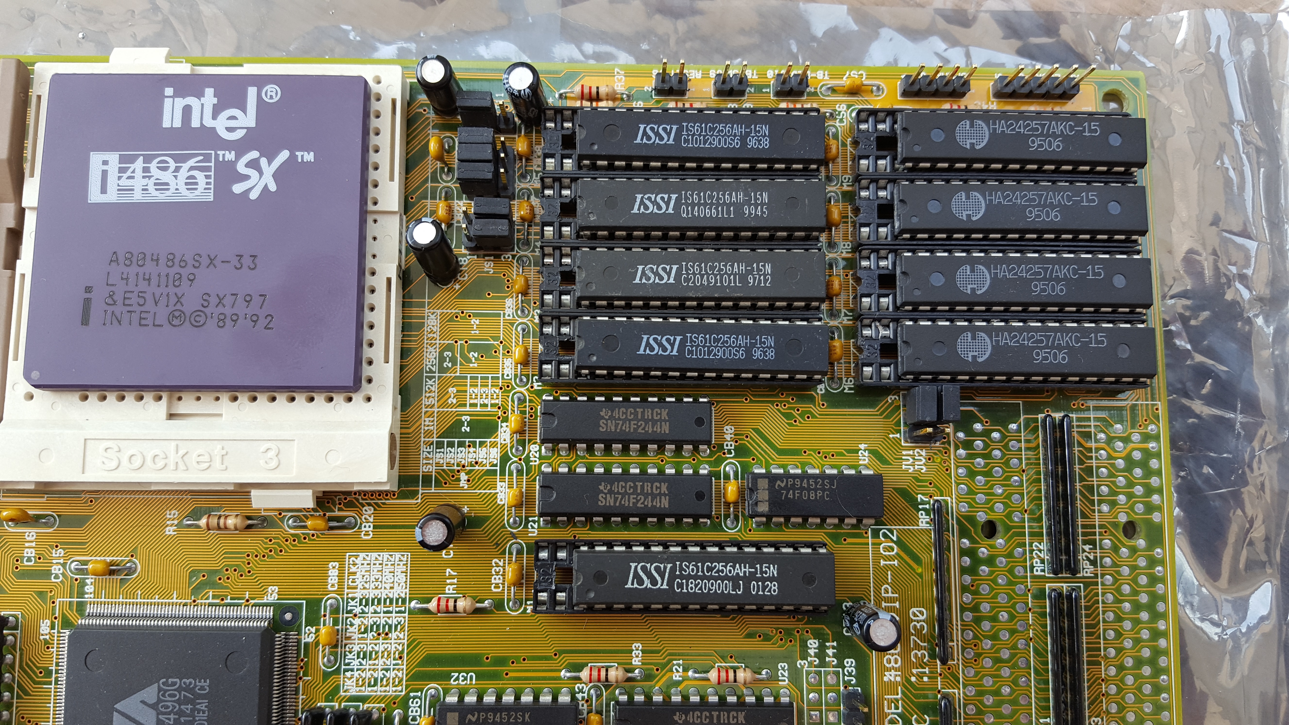
Click on the image for a higher-res version
My hope is that 256 KB of L2 cache is sufficient to make 64 MB of main memory cacheable. I did buy five ISSI IS61C1024-15N SRAM chips that would be suitable for this board to up it to 512 KB non-interleaved, but when installed some strange things started to happen: The Award BIOS' Hard Drive Detection option would always display an incorrect number of cylinders for my installed drive, and overriding them would just result in the Hard disk fail(80) message on boot-up. Maybe the chips I received are fake - I will do some more testing before giving up on them.
BIOS
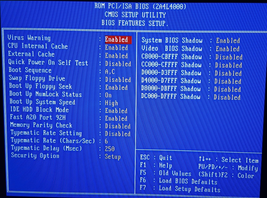
The motherboard comes with an Award Software core version 4.51PG 486DX BIOS. Mine here has BIOS version 5.12W2P(ES). This also appears on the initial POST screen:
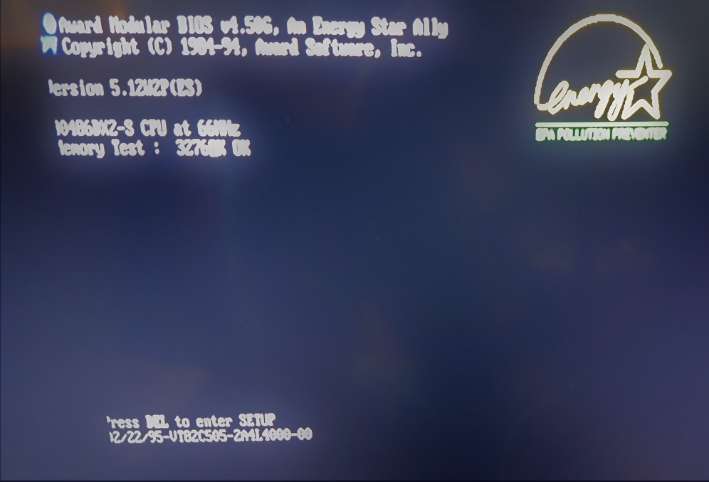
According to Ultimate Hardware, there are several later versions of the BIOS:
| Award | 05/28/96-VT496G-2A4L6F0IC-00 | 1.164G701 | 4.50PG | |
| Award | 02/21/97-VT496G-2A4L6F0IC-00 | 1.175G701 | 4.50PG |
Both of these fully support the P24T Pentium OverDrive processor with its internal WriteBack cache, as well as the AMD 5x86 133 MHz. My version number of 5.12W2P(ES) seems so far out from these ones, and is also over a year older, so further investigation will be required to work out what mine supports. At this stage I am assuming this was a bespoke version for a specific vendor.
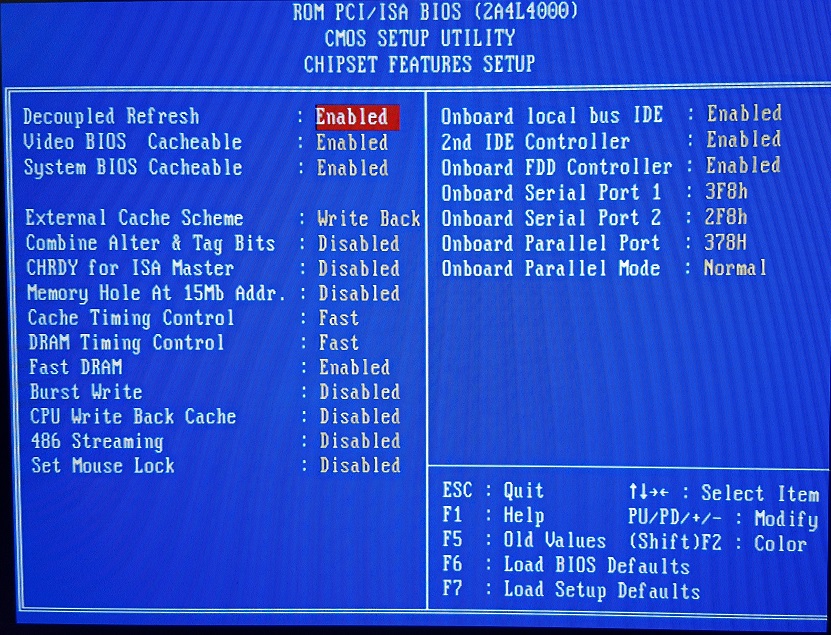
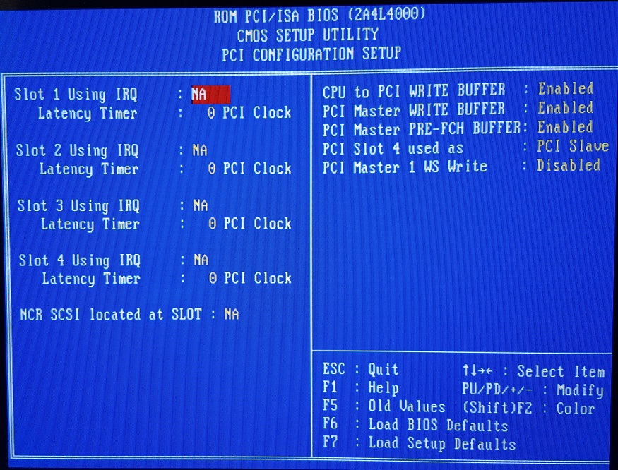
While the BIOS does have some performance-improving options under its Chipset menu, you cannot overclock the ISA bus, so it probably runs at the default of 8 MHz:
VESA Local Bus Slots
Some revisions of this motherboard come with the two VESA Local Bus slots in addition to the ISA and PCI, which is likely what the "VIP" stands for in the model number (Vesa, Isa, Pci). Mine unfortunately does not - just the solder pads. Since these are not 'through-hole' and it's most likely a multi-layered board, I don't feel too comfortable drilling through the pads and soldering in some third-party slots - let me know if you believe this is possible. Judging by pictures of boards that do have the slots in place, all other components appear to be in place on my board to support the VLB slots.
Head over to Part 2, where I begin on some improvements!
