Home 

IBM 5150  -  Motherboard Switch/Jumper Settings


On versus off

For the switches, some people are unsure about which position is on and which position is off.
If you are unsure, then click here to see examples.


Switch block SW1

Of SW1 and SW2, SW1 is the switch block closest to the center of the motherboard.
These settings apply to both the '16KB-64KB' and '64KB-256KB' versions of the 5150 motherboard.

Switch 1: 
OFF:  5150 has one or more floppy drives
ON:  5150 has no floppy drives
 • The ON setting was used for the floppy-less 5150s that IBM offered.
Switch 2: 
OFF:  8087 math co-processor chip is installed
ON:  8087 math co-processor chip is not installed
 • Some IBM documentation has this wrong.
 • 8087 sits in IC socket U4, adjacent to keyboard connector J7.
Switches 3 and 4:   
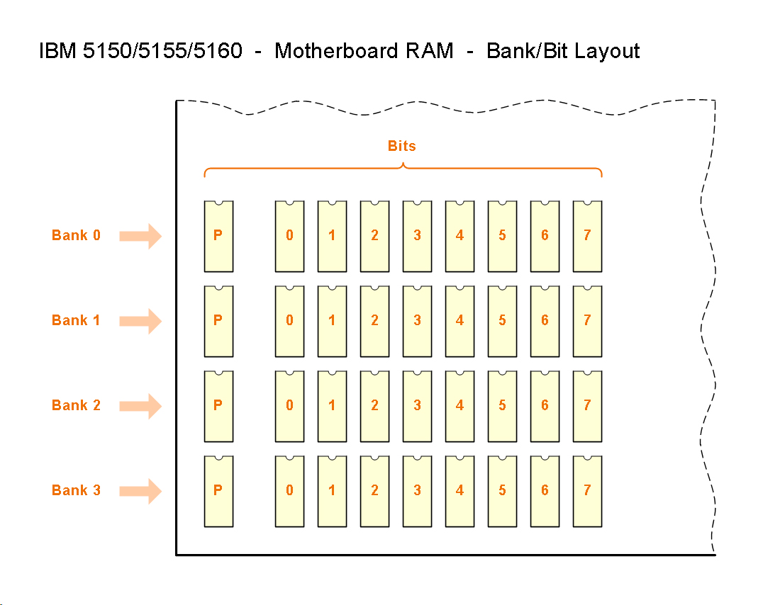
Installed motherboard RAM.
3=ON , 4=ON :  Only bank 0 populated
3=OFF, 4=ON :  Only banks 0/1 populated
3=ON , 4=OFF:  Only banks 0/1/2 populated
 3=OFF, 4=OFF:  Banks 0/1/2/3 populated
 • In a 5150, these switches do not enable/disable RAM.  They inform the BIOS of bank population.
 
 • Click here to see a diagram that shows the four RAM banks.
 
 • If the 10/27/82 dated BIOS revision is fitted, bugs in that  BIOS require that all four RAM banks be populated.
Switches 5 and 6:   Video card type.
5=OFF, 6=OFF:  MDA (monochrome)
5=OFF, 6=ON :  CGA, at 40 column by 25 line mode
5=ON , 6=OFF:  CGA, at 80 column by 25 line mode
5=ON , 6=ON :  Cards with a BIOS expansion ROM (e.g.  EGA / VGA)
 • Assumption: Only one video card fitted.

 • ON/ON setting is only useable for the 10/27/82 dated BIOS revision.

 • For VGA card compatibility, click here.
Switches 7 and 8:   Floppy drive count.   Used if switch 1 is OFF.
7=ON , 8=ON :  One floppy drive
7=OFF, 8=ON :  Two floppy drives
7=ON , 8=OFF:  Three floppy drives
7=OFF, 8=OFF:  Four floppy drives
 • The IBM 5.25" Diskette Drive Adapter supports double density drives only.


Switch block SW2

Of SW1 and SW2, SW2 is the switch block closest to the edge of the motherboard.

The SW2 switches are to be set to the total amount of conventional memory fitted in the 5150  (total = conventional on motherboard + conventional on expansion cards).
Basically, what you are doing with SW2, is informing the 5150's power-on self test (POST) of how much conventional memory that it should expect to find and test.

Warning: If you set SW2 to a lower amount that is actually fitted, the POST will only find and test that amount.  Consequently, DOS will only use that amount.

16KB-64KB type motherboard

For a 16KB-64KB motherboard, the SW2 settings vary according to the BIOS revision fitted to the motherboard.
Click here for information on how to identify the BIOS revision on a 5150 motherboard.
Once you know the BIOS revision level, use the SW2 settings diagram at here.

64KB-256KB type motherboard

For a 64KB-256KB motherboard, a diagram showing SW2 settings is here.


Jumper P4

For sending data to a cassette recorder, change the setting of jumper P4 according to whether the audio is going to either the:
1.  Cassette recorder's MICROPHONE jack; or
2.  Cassette recorder's AUXILIARY jack.

5150_cassette_jumper.jpg


Trimmer T1

On the PCB, labeled as "T1", and close by is "C.ADJ" - a shortened form of COLOUR ADJUST.
The trimmer is an adjustable capacitor.  The end of a small screwdriver fits into the slot on the top of the trimmer.

When using a composite monitor (or TV) as the display, adjusting the trimmer fine tunes the colours that appear.  Adjusting the trimmer does not affect the colours that appear on a digital monitor (MDA/CGA/EGA).

The trimmer's adjustable value is 5-30 pF.  If you need to replace the trimmer, and are having trouble finding a suitable replacement, then consider using a fixed value capacitor of say, 20 pF.  (Diagram)

Technical: Fine tunes the motherboard 14.31818 MHz clock signal, which in turn, fine tunes the NTSC 3.579545 MHz colour burst signal that the CGA card sends to the NTSC composite monitor.  (Diagram)

5150_t1.jpg