Home 

IBM 5160  -  Motherboard Switch/Jumper Settings


On versus off

For the switches, some people are unsure about which position is on and which position is off.
If you are unsure, then click here to see examples.


Switch block SW1

These settings apply to both versions of the 5160 motherboard, and apply to all three BIOS revisions for the 5160.

Switch 1: 
OFF:  Normal setting
ON:  Continuously perform the Power-On Self Test (POST)

 • ON: 'Test Chamber' mode - see here.
Switch 2: 
OFF:  8087 math co-processor chip is installed
ON:  8087 math co-processor chip is not installed
 • 8087 sits in IC socket U4, adjacent to power connectors.
Switches 3 and 4:   
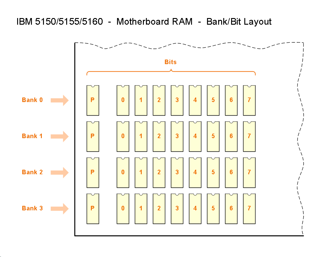
Enabled motherboard RAM.
3=ON , 4=ON :  Enable only bank 0
3=OFF, 4=ON :  Enable only banks 0/1
3=ON , 4=OFF:  Enable only banks 0/1/2
 3=OFF, 4=OFF:  Enable banks 0/1/2/3
 • Click here to see a diagram that shows the four RAM banks.
Switches 5 and 6:   Video card type.
5=OFF, 6=OFF:  MDA (monochrome)
5=OFF, 6=ON :  CGA, at 40 column by 25 line mode
5=ON , 6=OFF:  CGA, at 80 column by 25 line mode
5=ON , 6=ON :  Cards with a BIOS expansion ROM (e.g.  EGA / VGA)
 • Assumption: Only one video card fitted.

 • For VGA card compatibility, click here.

 • For PGC cards, see here.
Switches 7 and 8:   Floppy drive count.
7=ON , 8=ON :  One floppy drive
7=OFF, 8=ON :  Two floppy drives
7=ON , 8=OFF:  Three floppy drives
7=OFF, 8=OFF:  Four floppy drives
 • The IBM 5.25" Diskette Drive Adapter supports double density drives only.


Capacitor C1

The end of a small screwdriver fits into the slot on the top of the adjustable capacitor.

When using a composite monitor (or TV) as the display, adjusting the capacitor fine tunes the colours that appear.  Adjusting the capacitor does not affect the colours that appear on a digital monitor (MDA/CGA/EGA).

The capacitor's adjustable value is 5-30 pF.  If you need to replace the capacitor, and are having trouble finding a suitable replacement, then consider using a fixed value capacitor of say, 20 pF.  (Diagram)

Technical: Fine tunes the motherboard 14.31818 MHz clock signal, which in turn, fine tunes the NTSC 3.579545 MHz colour burst signal that the CGA card sends to the NTSC composite monitor.  (Diagram)

5160_c1.jpg


Jumper pad E1

If the pads of E1 are jumpered, that will completely disable both the U18 and U19 ROM sockets on the motherboard.
You would jumper E1 only if you were providing U18/U19 ROM functionality via an expansion card.

By "completely" above:
- The chip-select lines for the U18/U19 ROM sockets will never become active.
- If either the U18 or U19 ROM socket is addressed for a read, transceiver chip U15 will not drive the data bus.
- A related diagram is at here.


Jumper pad E2 - pins 1 and 2

Jumpering/joining pins 1 and 2 of jumper pad E2, is one of the possible ways of grounding pin 1 on chip U44.

The grounding of pin 1 on U44 was done as part of the process of putting 640 KB of RAM on a 64-256KB motherboard.  See note 1 at the bottom of here.


Jumper pad E5

Per here, jumper pad E5 is part of the keyboard interface circuitry.

Per here, pins 2 and 3 of E5 are connected by a wide trace on the underside of the PCB.
Should someone (?) decide to cut that trace, followed by connecting pins 1 and 2 together, then pin PB2 of the 8255 chip will control (via chip U85) the data line of the keyboard connector.
At one time, IBM must have seen reason to allow that.

But, with jumper pad E5 wired as default (pins 2 and 3 connected), pin PB2 of the 8255 is unused ('spare'), free for custom use - see here.