| Home |
| Step | Action | Comment | Reference |
|---|---|---|---|
| 0 | DISABLE MASKABLE INTERRUPTS | At the CPU | Page 5-34 (line 310) |
| 1 | 8088 CPU TEST | If the test fails, halt the CPU. | Page 5-34 |
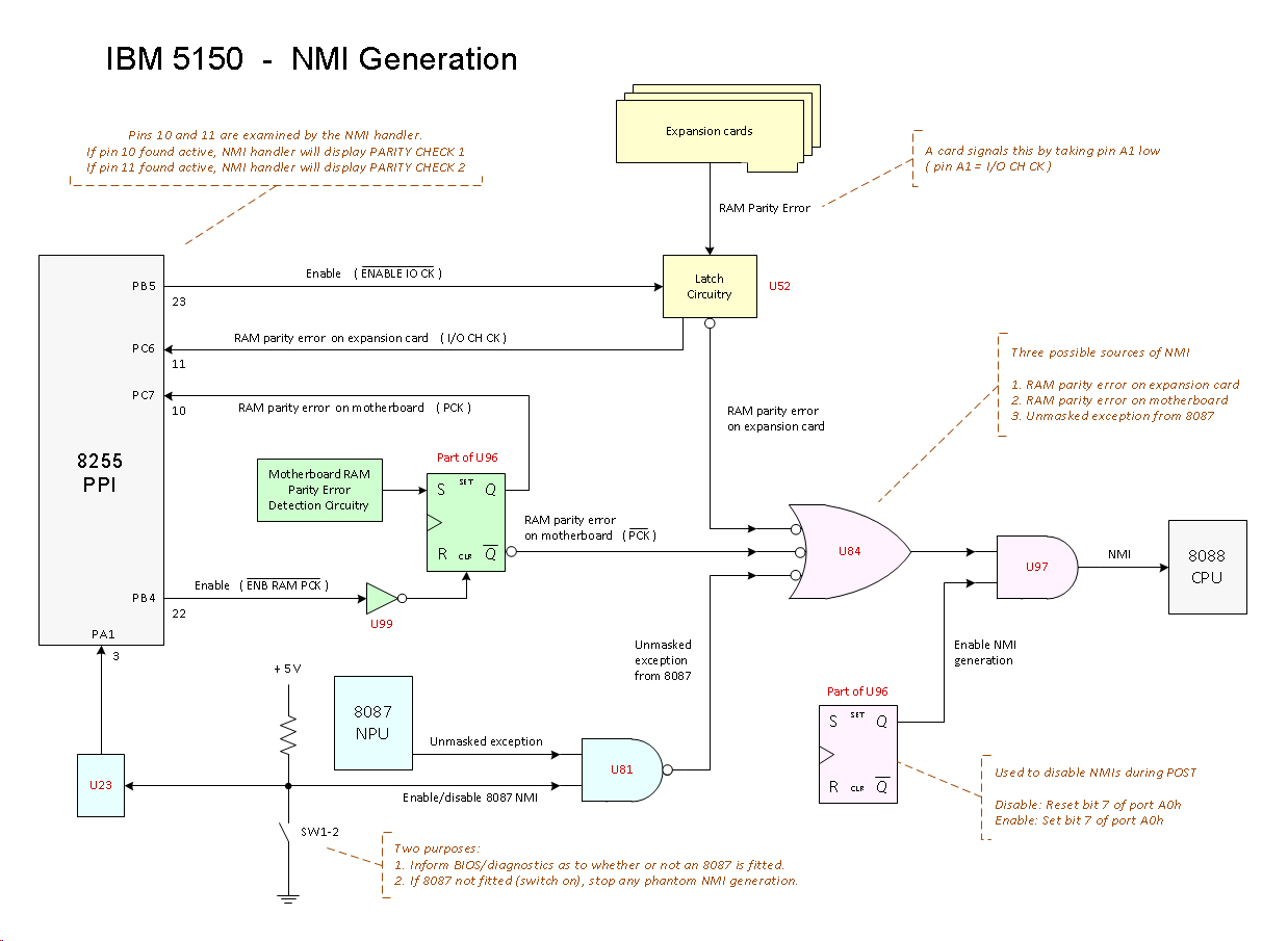
| 2 | DISABLE NON-MASKABLE INTERRUPTS | Disable non-maskable interrupts (NMIs) from reaching the CPU. A diagram is here. | Page 5-35 (line 370) |
| 3 | DMA CHAN 0/1 PAGE REGISTER | Zero the page register used by DMA channels 0 and 1. See note 15. | Page 5-35 (line 371) |
| 4 | DISABLE VIDEO | Page 5-35 (lines 372-376) | |
| 5 | 8255 OPERATION | 8255 PPI chip. Set port B lines to outputs. See note 11 for more info. | Page 5-35 (lines 377-378) |
| 6 | 8255 OUTPUTS | Set the 8255's port B lines to various states. | Page 5-35 (lines 379-380) |
| 7 | ROM CHECKSUM TEST I | Verify that the 8-bit checksum of the BIOS ROM, U33, is 00. If verification fails, halt the CPU. (U33 = 8 KB block at FE000) | Page 5-35 (lines 381-390) |
| DISABLE DMA CONTROLLER | Disable the 8237 DMA controller chip. | Page 5-35 (lines 399-400) | |
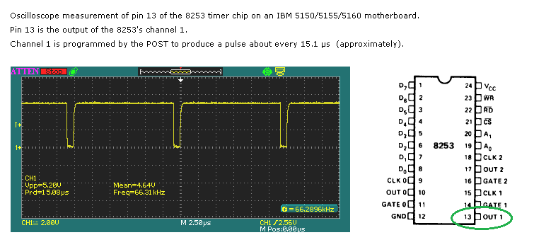
| 8 | TEST TIMER 1 | Channel #1 on 8253 timer chip. Channel #1 is used in RAM refresh process. If the test fails, halt the CPU. | Page 5-35 (lines 402-430) |
| 9 | INITIALIZE TIMER 1 | Channel #1 on 8253 timer chip. Set a divisor of 18. That results in one output pulse per approx. 15 µs. See here. | Page 5-35 (lines 435-436) |
| 10 | TEST DMA CONTROLLER | Test the 8237 DMA controller chip. If the test fails, halt the CPU. | Page 5-36 (lines 439-462) |
| 11 | START RAM REFRESH | Initialise and start DMA for RAM refresh (RAM refresh done via dummy DMA transfers). | Page 5-36 (lines 464-486) |
| 12 | EXPANSION I/O BOX - ENABLE | Write 1 to port 213h. If an extender card for the IBM 5161 Expansion Unit is present in the 5150, that action enables the extender card to
communicate with the 5161. Presumably, this enabling is done now so that any RAM in the 5161 is zeroed in step 15. See note 6 for more information. |
Page 5-36 (lines 498-500) |
| 13 | BASE 16 KB RAM TEST | If a cold boot, test the first 16 KB of RAM. If the test fails, halt the CPU. | Page 5-36 (lines 502-508) |
| 14 | ZERO MOTHERBOARD RAM UP TO 64 KB |
Size determined by examination of switches 3/4 on switch block SW1. Assumes that RAM banks on motherboard are 16 KB sized. See note 7. Done on both cold and warm boots. For cold boots, the act of writing to each RAM address will appropriately set/reset the parity bit of each address. See note 5. |
Page 5-36 (lines 509-520) |
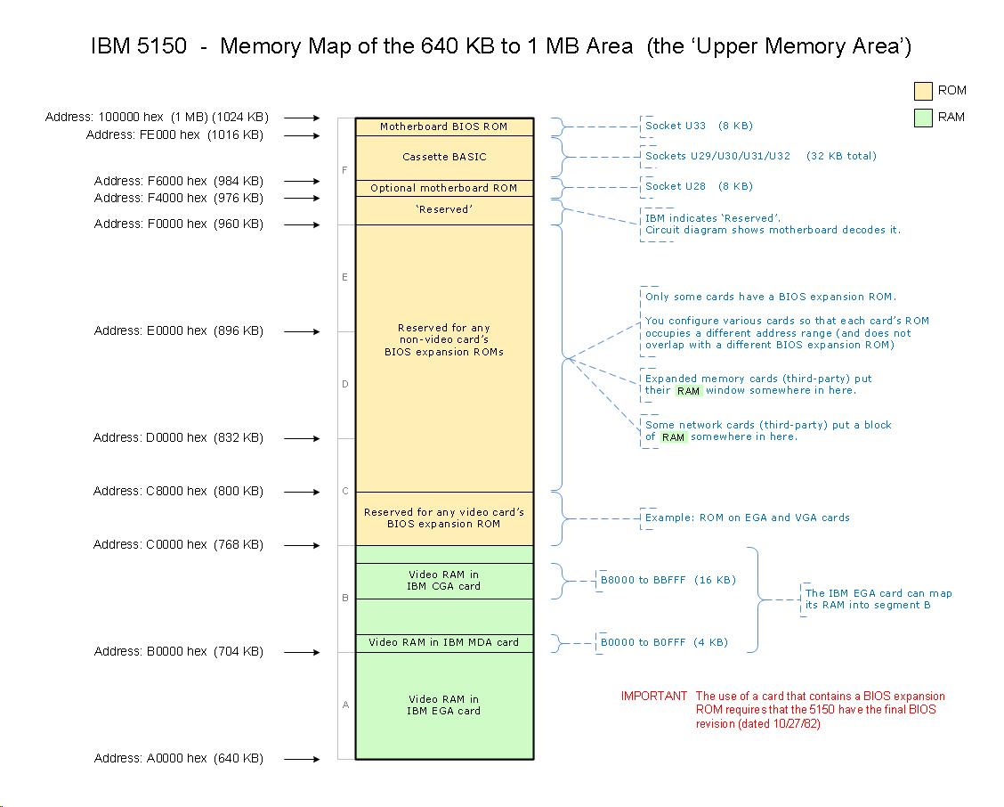
| 15 | ZERO RAM PAST 64 KB | Conventional memory only. Upper limit determined by examination of switches 1 to 5 on switch block SW2. See note 8. Done on both cold and warm boots. For cold boots, the act of writing to each RAM address will appropriately set/reset the parity bit of each address. See note 5. This code contains a bug. See note 10. |
Page 5-37 (lines 525-551) |
| 16 | 8259 INITIALISATION | Initialise the 8259 interrupt controller chip. | Page 5-37 (lines 556-563) |
| 17 | SET UP STACK SEG AND SP | Set up the stack segment and stack pointer. | Page 5-37 (lines 570-572) |
| IF REQUESTED, LOAD DIAG. CODE | Take the clock pin in the motherboard's keyboard DIN connector LOW for 20 ms. (Done by the KBD_RESET subroutine.) If the attached device responds with the byte of 65h, the attached device is a special IBM device that supplies diagnostic/test code to the 5150 via the keyboard port. If 65h received, load in the diagnostic/test code (255 bytes) via the keyboard port, then execute the code. |
Page 5-37 (lines 575-592) | |
| 18 | 8259 TEST | 8259 interrupt controller chip. Step 18.1: Test the IMR register. Step 18.2: Look for hot interrupts. If the test fails, beep 1 long then 1 short, then halt the CPU. NOTE: This is a very limited test of the 8259. |
Page 5-38 (lines 622-651) |
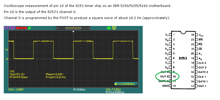
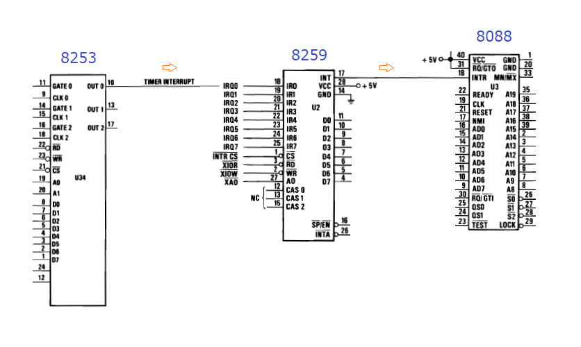
| 19 | TEST/SET TIMER 0 | Channel #0 on 8253 timer chip. This is what generates IRQ 0 (system timer). Verify that channel #0 does not count too fast or too slow. If the test fails, beep 1 long then 1 short, then halt the CPU. If the test passes, set channel #0 output to a square wave of approx. 18.2 Hz. See here. NOTE: The test relies on the ability of the 8259 to process IRQ 0 and the ability of the 8088 to process interrupts from the 8259. See here. |
Page 5-38/39 (lines 659-705) |
| DETECT IF MANUFACTURING TEST MODE |
If the keyboard data line is grounded, then: Step 1: Set the 'Manufacturing Test' flag. See here. Step 2: "BLINK LED" on IBM's test kit. See here. |
Page 5-39 (lines 709-725) | |
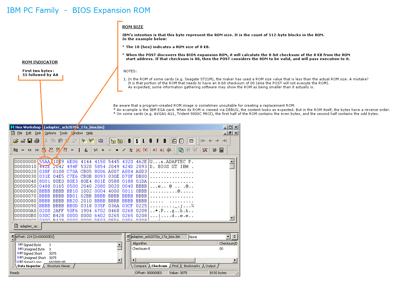
| 20 | INIT/START VIDEO CONTROLLER | Examine video switches on motherboard (SW1:5 and SW1:6) to see which type of video card is selected. STEP 1 OF 2: If MDA or CGA selected, then look for that type of card. If card not found, beep 1 long then 2 short. If card found, try to initialise the card. If there is a problem found when initialising the card, beep 1 long then 2 short. (Because of a bug, 1 long then 2 short beeps can also occur in step 27.) STEP 2 OF 2: Irrespective of the type of video card selected, look for BIOS expansion ROM's in address block C0000 - C7FFF. Those will be video ROM's in EGA/VGA cards. If one found (first 2 bytes are 55/AA), verify that its 8-bit checksum is 00, and if that verification passes, call the initialisation code in the ROM. If the verification fails, then display the segment address of faulty ROM followed by "ROM" (e.g. "C000 ROM"). See note 4 for more information. |
Pages 5-39 to 5-41 |
| 21 | EXPANSION I/O BOX - TEST | If an extender card for the IBM 5161 Expansion Unit is fitted in the 5150, then test communications with the 5161. If the test fails, display an "1801" error. See the 1801 section of here. |
Page 5-41 |
| 22 | CALCULATE TOTAL RAM | Calculate the total amount of conventional memory. This code contains a bug. See note 9. |
Page 5-42 (lines 934-951) |
| 23 | ADDITIONAL RAM TEST | If a cold boot, test the conventional memory past 16 KB. If the test fails, display the number (in hex) of the failing 4 KB block followed by bit error pattern, followed by " 201". Example: "0510 201". Click here for detailed information. |
Page 5-42 (lines 952-998) |
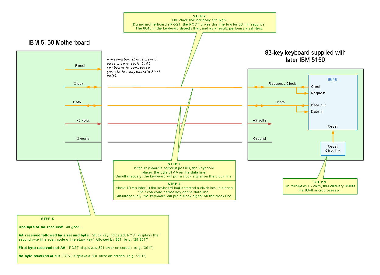
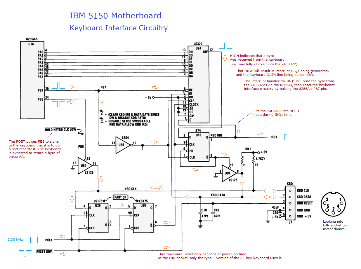
| 24 | KEYBOARD TEST | Diagram here. If there is a problem, display a "301" error. See note 13 for possible 301 causes. NOTE: This test is skipped if the POST is in 'Manufacturing Test' mode. |
Page 5-43 |
| 25 | INTERRUPT VECTORS | Set up the interrupt vector table. | Page 5-43 (lines 1034-1049) |
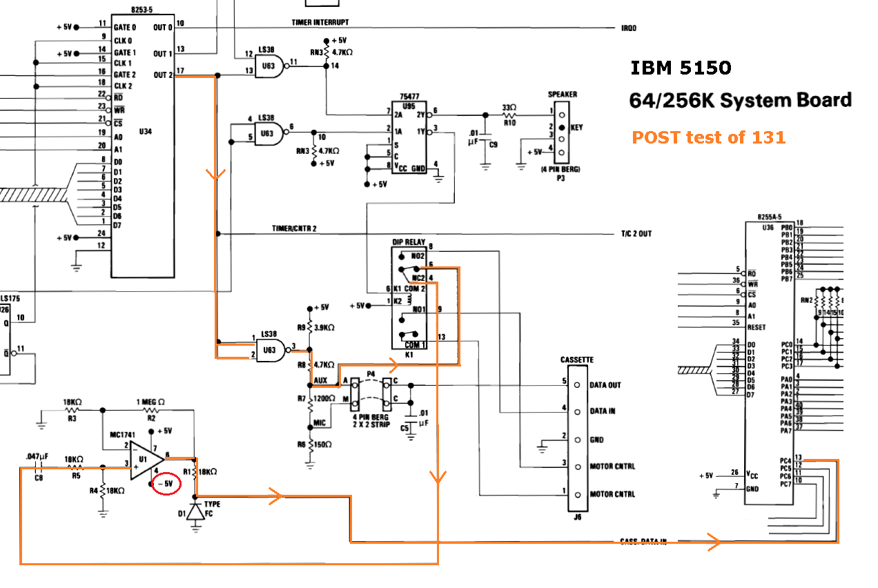
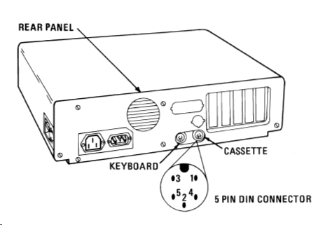
| 26 | CASSETTE PORT - INTERNAL WRAP/LOOPBACK TEST |
With the cassette relay (K1) in its default state of off, the POST should receive from the cassette circuitry what the POST sends to it. A diagram is here. If the test fails, display a "131" error. See note 12 for possible causes. |
Page 5-44 |
| 27 | EXPANSION ROM SEARCH | Look for BIOS expansion ROM's in address block C8000 - F5FFF (see note 3). For each one found (first 2 bytes are 55/AA), verify that the 8-bit checksum of the ROM (size is in third byte) is 00. More info here. If verification passes, call the initialisation code in the ROM. If verification fails, then display the segment address of faulty ROM followed by " ROM" (e.g. "D000 ROM"). BUG: Because of a bug, if the faulty ROM starts at C8000 (which is the norm for an XT class hard disk controller), instead of "C800 ROM" being displayed, there will be 1 long beep then 2 short beeps. See note 2 for more information. |
Page 5-44 See note 1 for more info. |
| 28 | ROM CHECKSUM TEST II | Step 28.1: Verify that the 8-bit checksum of BASIC ROM U29 is 00. If not 00, display "F600 ROM". Step 28.2: Verify that the 8-bit checksum of BASIC ROM U30 is 00. If not 00, display "F800 ROM". Step 28.3: Verify that the 8-bit checksum of BASIC ROM U31 is 00. If not 00, display "FA00 ROM". Step 28.4: Verify that the 8-bit checksum of BASIC ROM U32 is 00. If not 00, display "FC00 ROM". |
Page 5-44 |
| LOOP POST IF REQUIRED | See if at least one floppy drive is present, by examining switch 1 on switch block SW1. If no floppy drives are indicated (i.e. switch 1 is ON), and the POST is in 'Manufacturing Test' mode, then restart the computer. |
Page 5-45 (lines 1141-1146) | |
| 29 | FLOPPY (DISKETTE) DRIVE ATTACHMENT TEST |
Step 29.1: Test communication with floppy controller card. On failure, display a "601" error. Step 29.2: Via controller, turn on spindle motor of floppy drive 0. Step 29.3: Via controller, with 'RECAL REQUIRED' set, move heads of floppy drive 0 to track 1. On failure, display a "601" error. Step 29.4: Via controller, with 'RECAL REQUIRED' set, move heads of floppy drive 0 to track 34. On failure, display a "601" error. Step 29.5: Via controller, turn off spindle motor of floppy drive 0. This test can pass if head stepping is not happening properly - see note 14. NOTE: 'RECAL REQUIRED' tells the controller that before it moves the heads to the target track, it is to first move the heads back to track 0. NOTE: After successful execution, the heads are left at track 34. At POST end, the heads will go back to track 0 as part of a boot attempt. NOTE: When DOS later loads (step 38), DOS will assign drive letter A (a logical drive) to floppy drive 0 (a physical drive). NOTE: This test is skipped if switch 1 on switch block SW1 is in the ON position. |
Page 5-45 |
| 30 | SET UP KEYBOARD BUFFER | Page 5-45 (lines 1188-1194) | |
| 31 | 8259 - ENABLE TIMER/KYB INT | 8259 interrupt controller. Enable interrupts IRQ 0 (system timer) and IRQ 1 (keyboard). | Page 5-45 (lines 1195-1197) |
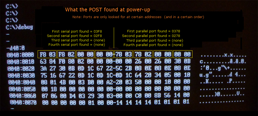
| 32 | DETERMINE LPT (PARALLEL) PORTS | Check for parallel ports at the following I/O addresses, in that order: 3BC, 378, 278 When a port is found, put the base address of the port into the BIOS Data Area (see here). |
Page 5-45 (lines 1198-1216) |
| 33 | DETERMINE COM (SERIAL) PORTS | Check for serial ports at the following I/O addresses, in that order: 3F8, 2F8 When a port is found, put the base address of the port into the BIOS Data Area (see here). |
Page 5-45 (lines 1217-1241) |
| 34 | JOYSTICKS | Are two joysticks present? See here | Page 5-46 (lines 1242-1246) |
| 35 | SET LPT/COM TIMEOUTS | Page 5-46 (lines 1249-1259) | |
| 36 | ENABLE NON-MASKABLE INTERRUPTS | A diagram is here. | Page 5-46 (lines 1263-1264) |
| 37 | BEEP 1 SHORT TONE | NOTE: This beep is not done if the POST is in 'Manufacturing Test' mode. | Page 5-46 (lines 1267-1268) |
| 38 | DO BOOTSTRAP | Essentially, the boot order is: 1. floppy drive 0 (if switch 1 on motherboard SW1 is OFF) 2. hard drive 0 (if XT-class hard disk controller present) 3. cassette BASIC |
Page 5-46 (line 1271) |
| Note 1 | Page 5-124: ROM_SCAN - The code that does the search. Page 5-169: ROM_CHECK - The code called to see if a particular ROM has an expected 8-bit checksum of 00. Page 5-126: ROM_ERR - The code called if a ROM's 8-bit checksum is bad (not 00). |
| Note 2 | The bug is in routine ROM_ERR (page 5-53 of reference). One of the things this routine does is determine if the bad ROM (bad = 8-bit checksum not 00) is either: 1. A video ROM; or 2. Some other type of BIOS expansion ROM. It does that by examination of DS. If DS is less than C800, a video ROM is indicated. The bug is that "JLE ROM_ERR_BEEP" has been used instead of "JL ROM_ERR_BEEP". Bug verified using a simulated corrupt ROM (EPROM with tenth byte altered) in an NDC5127 MFM controller. The bug does not appear in the BIOS of the IBM 5160. |
| Note 3 | Start signature of ROM checked for in 2 KB increments: C8000, C8800, C9000, --> F5800 The last address checked is F5800, which makes sense because cassette BASIC starts at F6000. Diagram here. Block end address incorrectly commented as "F4000" in source code. It should be "F6000". Note that any ROM placed in socket U28 is included in the search. Diagram here. |
| Note 4 | * The search for EGA/VGA video ROM's always happens, even if the motherboard's video switches are set for MDA or CGA. * EGA/VGA cards initialise themselves, via initialisation code in their ROM. * The initialisation code in some video ROM's produce their own error beeps. Example: IBM EGA cards can produce 1 long beep followed by 3 short beeps. |
| Note 5 | On power on of the computer, the contents of motherboard RAM will be somewhat random. That means that for a certain portion of addresses, the content of the parity bit will not reflect the parity of the combined data bits. After POST completion (non-maskable interrupts enabled), attempts to read from such addresses would result in a parity error. By writing (anything) to the addresses now, the parity bit at the address is appropriately set/reset. |
| Note 6 | This step may not actually be required because in the IBM documentation on the IBM 5161 is, "The expansion unit is automatically enabled upon power-up." But maybe the "expansion unit" in that sentence excludes the cable and extender card. This step disappears when the 01/10/86 revision of the IBM 5160 BIOS is introduced. |
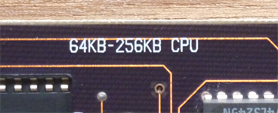
| Note 7 | Even though on the 64KB-256KB motherboard, where the RAM banks are 64 KB sized, this routine assumes that RAM banks on motherboard are 16 KB sized. If switches 3/4 set to on/on (bank 0), calculated motherboard RAM is 16 KB. If switches 3/4 set to off/on (banks 0/1), calculated motherboard RAM is 32 KB. If switches 3/4 set to on/on (banks 0/1/2), calculated motherboard RAM is 48 KB. If switches 3/4 set to off/off (banks 0/1/2/3), calculated motherboard RAM is 64 KB. |
| Note 8 | What is calculated, and stored in IO_RAM_SIZE for later use, is the KB size of RAM past 64 KB. Example: If SW2 settings are set for 256 KB, calculated for IO_RAM_SIZE is 192 KB. By "IO_RAM", IBM means RAM on expansion cards. Therefore, when this BIOS is on a 16KB-64KB motherboard, "IO_RAM" is a proper description. But when this BIOS is on a 64KB-256KB motherboard, the use of "IO_RAM" is incorrect. Instead of "IO_RAM_SIZE", IBM should have used something like "RAM_PAST_64K". |
| Note 9 | The bug only presents a problem if less than 4 banks of motherboard RAM are populated. For more information, read the BUG #1 section in 5150_27OCT82_less_than_4_ram_banks.htm |
| Note 10 | The bug only presents a problem if less than 4 banks of motherboard RAM are populated. For more information, read the BUG #2 section in 5150_27OCT82_less_than_4_ram_banks.htm |
| Note 11 | At power on (and after RESET released), the 8255 defaults to mode 0 operation for both groups, with all 3 ports (A, B and C) being inputs. So, even though the command sent to the 8255 is [Group_A_mode=0, Group_B_mode=0, Port_A=inputs, Port_B=outputs, Port_C_upper=inputs, Port_C_lower=inputs], the only result is that the port B lines change from inputs to outputs. |
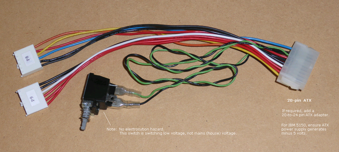
| Note 12 | Some possible 131 causes: 1. Motherboard of type 64KB-256KB is not receiving minus 5 volts. • Try reseating plug P9 from power supply, in case of bad connection. • Perhaps in use is an ATX power supply (via adapter) that does not have a minus 5 volts output. 2. Motherboard relay K1 (cassette relay) is stuck in the 'motor on' position (indicated by zero, or low, resistance between pins 1 and 3 of the cassette DIN connector). 3. Faulty motherboard. |
| Note 13 | If the "301" is preceeded by a byte, e.g. "23 301", then the keyboard's self test is indicating to the POST that a key is 'stuck' down. The byte indicates which key (see here). If the "301" is not preceeded by a byte, then it's a general keyboard error. Possible causes: 1. AT class keyboard attached. That will not work. A PC/XT class keyboard is required. 2. Keyboard accidentally attached to cassette connector instead of keyboard connector. 3. No keyboard attached. 4. Faulty keyboard - broken wire in cable. 5. Faulty keyboard - wire loose in connector. 6. Faulty keyboard - chip failure. 7. Faulty motherboard - bad solder joint on DIN connector for keyboard. 8. Faulty motherboard - some cases of faulty keyboard circuitry. |
| Note 14 | The only form of head position feedback that the floppy drive electronics has, is a switch that detects whether or not the heads are at the first track, track 0. And so the drive really doesn't know if the heads got as far as track 34. For example, deteriorated lubrication on the drive's rails (resulting in improper head stepping) may mean that the heads only got as far as say, track 22. In that example, the drive is faulty (improper head stepping), but the 601 test is passing because the drive is unable to detect exact head position (except for the heads being on track 0). |
| Note 15 | Looking at the circuit diagram of the IBM 5150 motherboard: • Chip U19, a 74LS670, contains four page registers. • Page register 0 (mapped to port 80h) is unused (RB and RA cannot be 0 at the same time, because /DACK2 and /DACK3 cannot be 0 at the same time) • Page register 1 (mapped to port 81h) is used by DMA channel 2 (RB=0 and RA=1, because /DACK2=0 and /DACK3=1) • Page register 2 (mapped to port 82h) is used by DMA channel 3 (RB=1 and RA=0, because /DACK2=1 and /DACK3=0) • Page register 3 (mapped to port 83h) is used by DMA channels 0 and 1 (in both cases, RB=1 and RA=1, because /DACK2=1 and /DACK3=1) |