| Home |
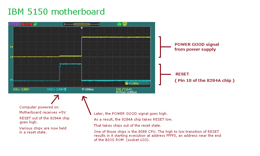
| 1. | User turns on power supply. |
| 2. | Motherboard receives +5 volts from the power supply. |
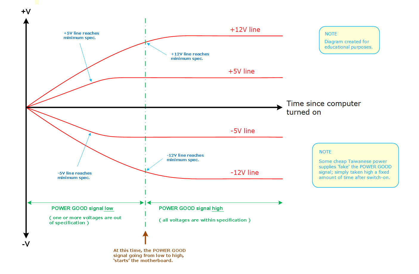
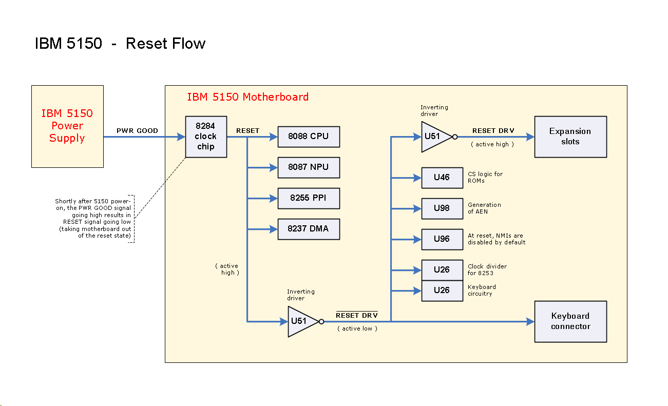
| 3. | Also received from the power supply is the POWER GOOD signal, a digital signal of TTL levels, which at this time, is low. <----- Important: At this time, the signal is LOW |
| 4. | Because the POWER GOOD signal is low, the motherboard's 8284A chip takes the motherboard's RESET line high. Per here, various chips on the motherboard (including the 8088 CPU) are held in a reset state. |
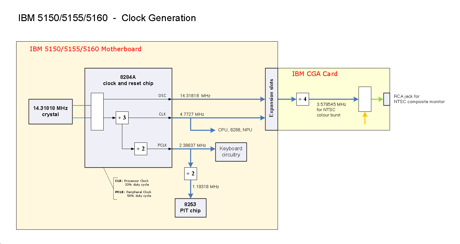
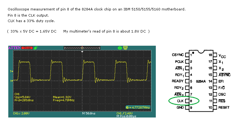
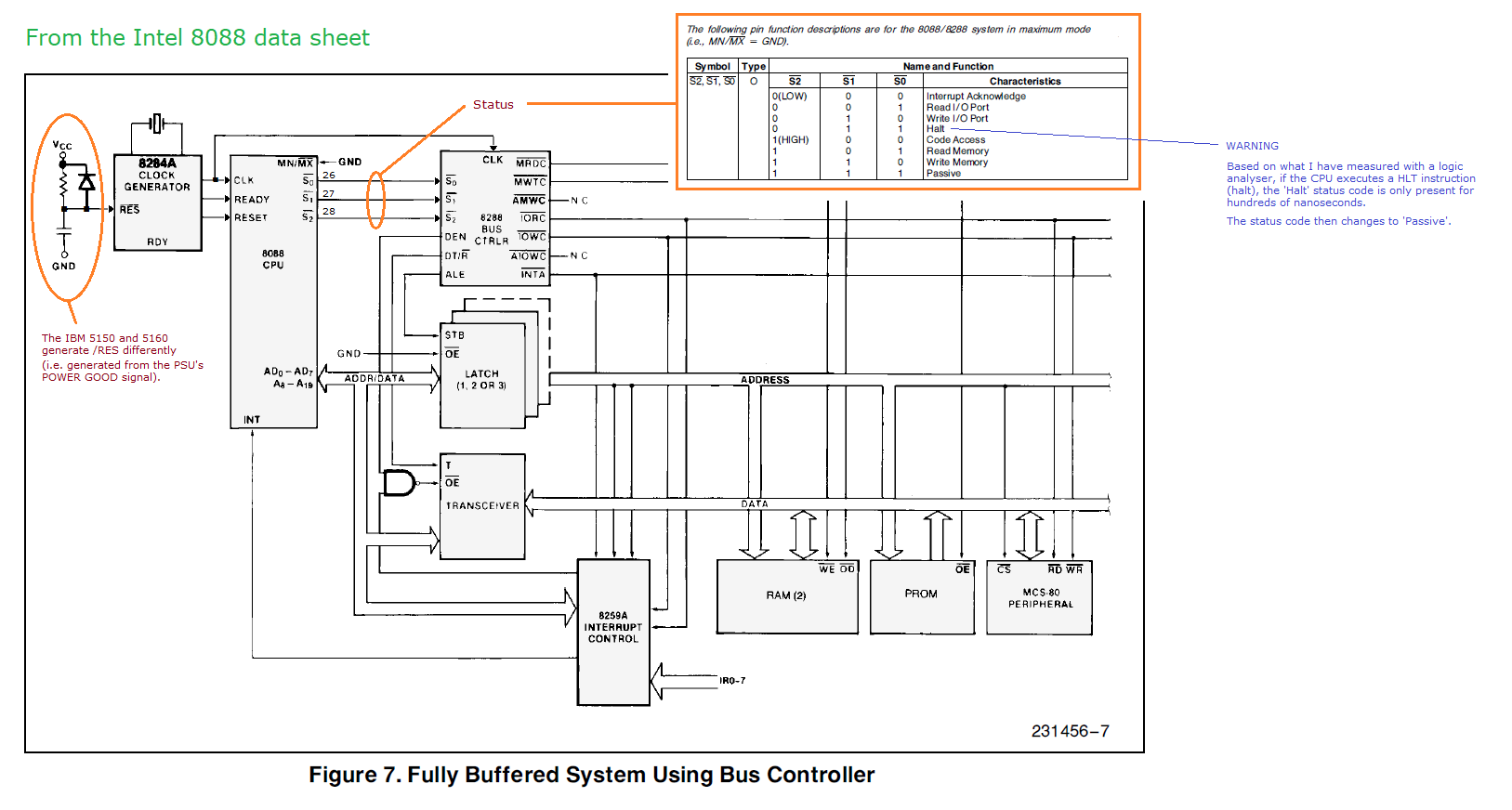
| 5. | Refer to here. On the motherboard, the 8284A chip generates a 4.7727 MHz clock signal for the 8088 CPU and the 8288 bus controller chip. (And optional 8087 NPU, if fitted.) |
| 6. | Later, when all voltages from the power supply are within specification, the power supply takes the POWER GOOD line high. Pictured at here. |
| 7. | When the 8284A chip sees the power supply's POWER GOOD signal go high, it takes the motherboard's RESET line from high to low. As a result, chips are taken out of the reset state. |
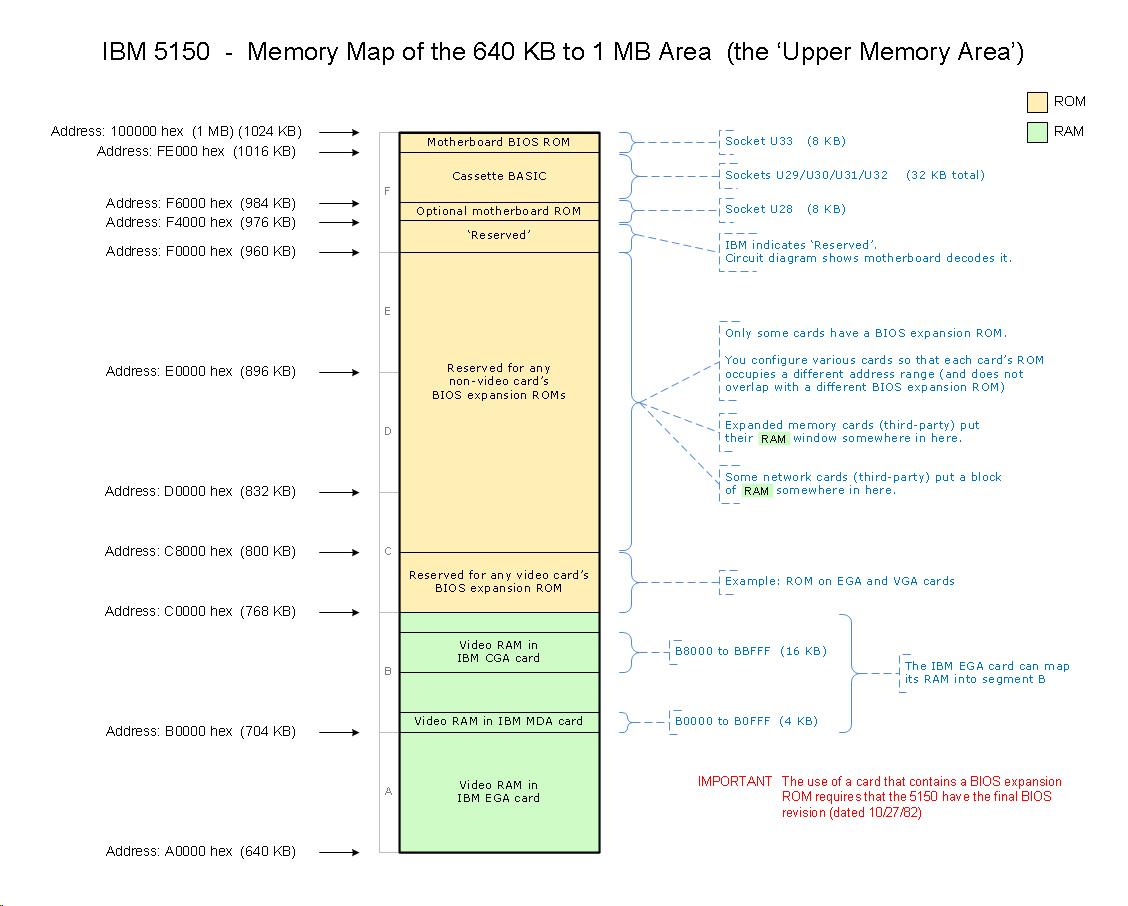
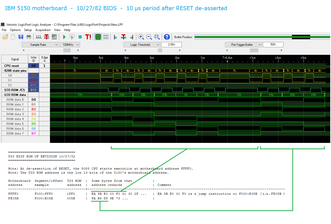
| 8. | When the 8088 CPU leaves the reset state (see note 1 below), it starts execution at address FFFF0. In the IBM 5150, that address corresponds to an address near the end of motherboard ROM chip U33, the motherboard's BIOS ROM (per here). |
|
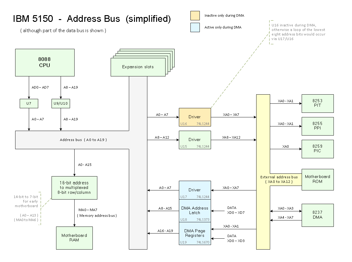
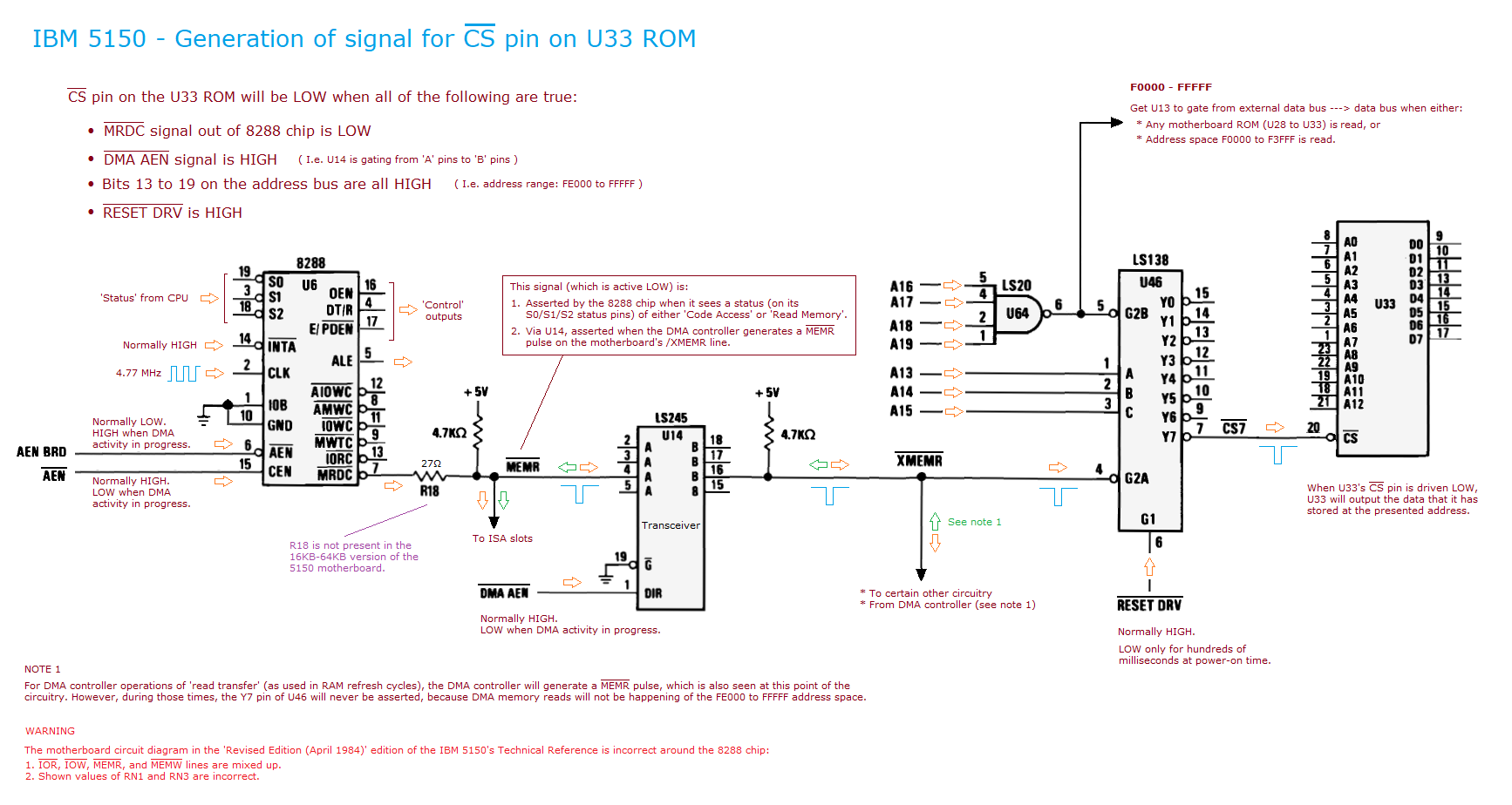
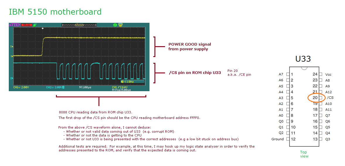
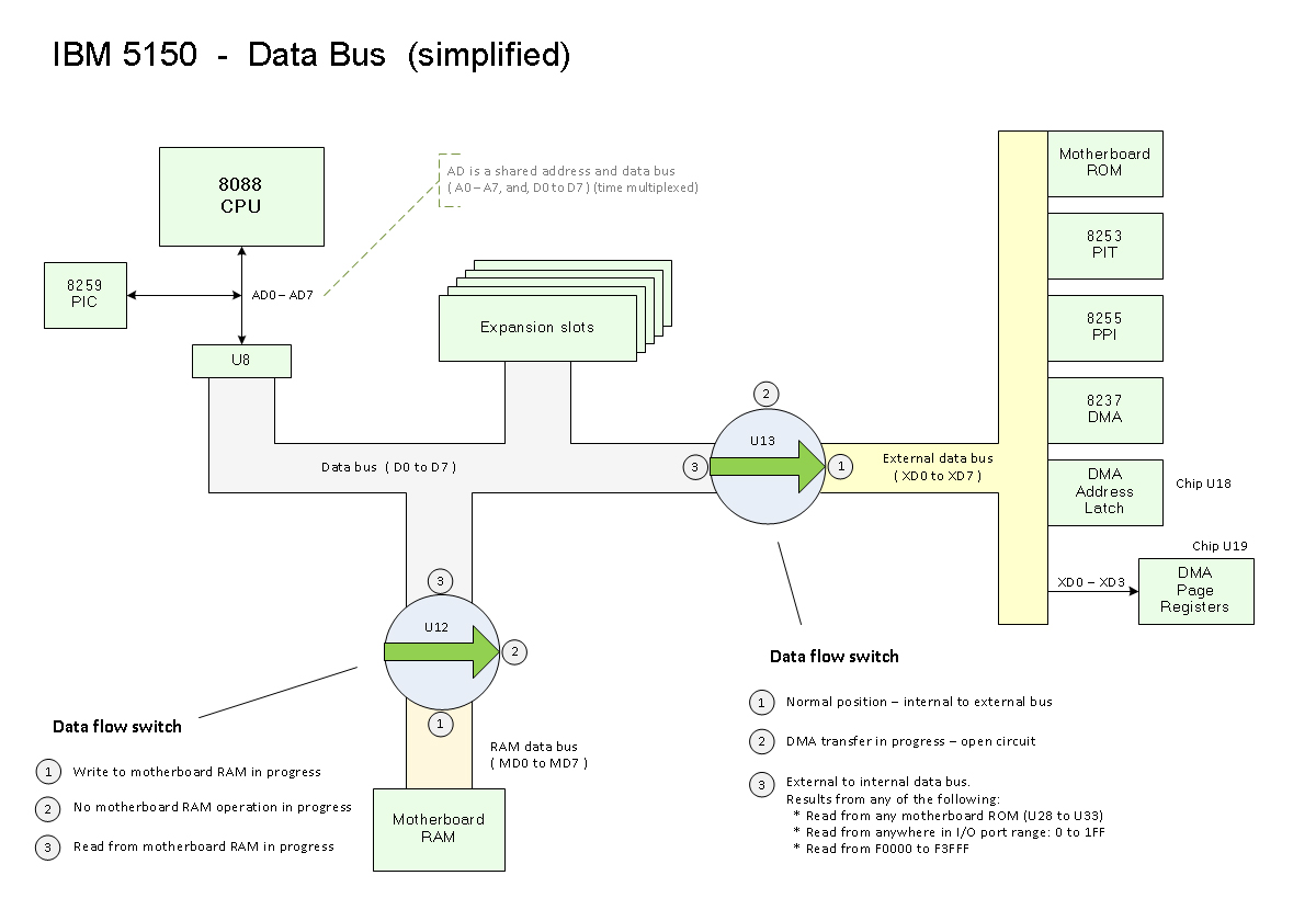
Basically (repeat: basically), the read of address FFFF0 goes something like: - 8088 starts a 'Code Access' bus transaction. - 8088 sets its three status pins (see here) to indicate to the 8288 chip that a 'Code Access' bus transaction is in progress. - The 8288 chip, seeing the 8088 indicate a status of 'Bus Access', asserts its /MRDC output pin. - - Per here, the 8088, and certain circuitry, outputs address FFFF0 onto the address bus. - The low 13 bits of the address bus are put onto the external address bus by driver chips U15 and U16. - The 13 address pins of ROM chip U33, which are on the external address bus, see address 1FF0 (the low 13 bits of address FFFF0). - - Certain circuitry establishes that motherboard address FFFF0 corresponds to ROM chip U33, and accordingly, drops the /CS pin (/CE pin) on ROM chip U33. See here and here. - As a result, ROM chip U33 outputs the data it has at its 1FF0 address onto the external data bus. - Certain circuitry instructs U13 to put that data from the external data bus onto the data bus. - Per here, the 8088 reads the data bus. BTW. If you have a logic probe (or multimeter), you can see that for yourself via the procedure at here. |
|
| 9. | Starting at ROM chip U33's address of 1FF0, are five bytes, which together form a jump instruction to the start of the BIOS' power-on self test (POST). At here is a capture of that via a logic analyser. |
|
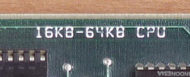
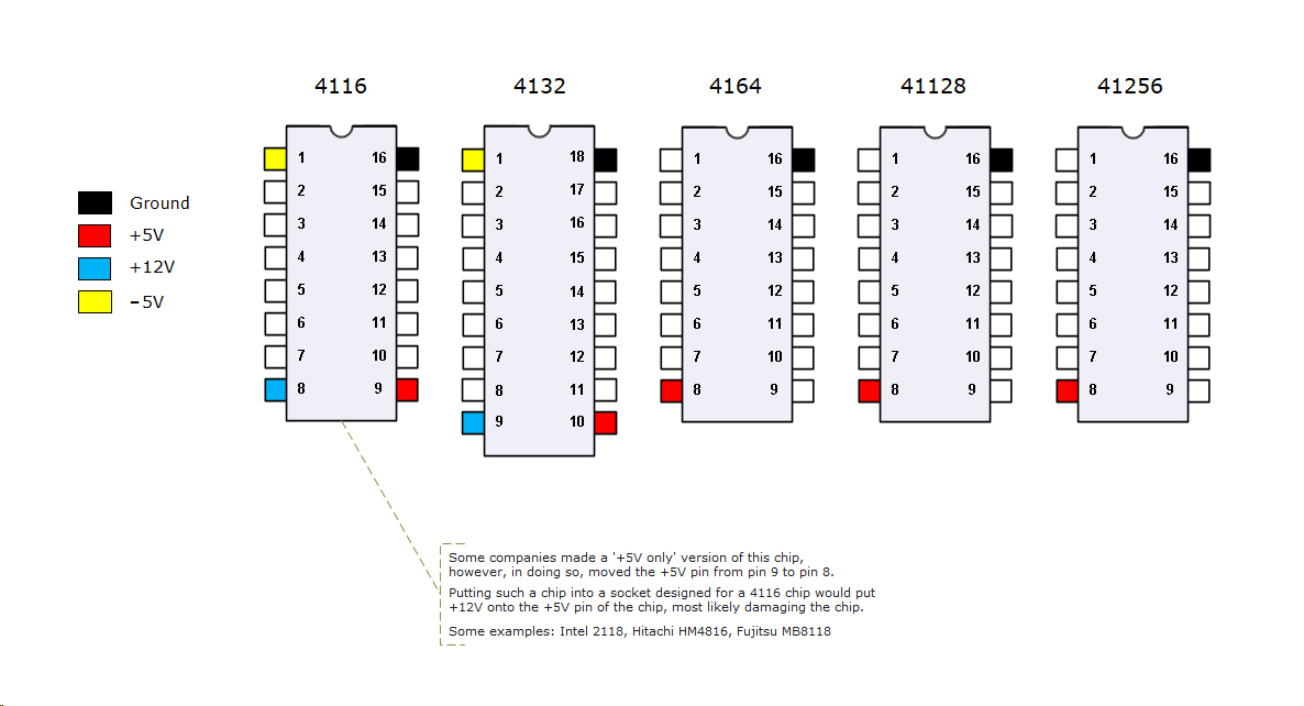
It needs to be noted that past this point, the 16KB-64KB revision of the IBM 5150 motherboard also requires -5V and +12V, for its 4116 class RAM chips. If either -5V or +12V are not reaching the 4116 RAM chips, the POST's check of the first 16K of RAM will fail (and you will get absolutely no indication). |
|
| 10. | The POST executes. Details are at here. |
| Note 1 | The data sheet for the Intel 8088 indicates that there is minimum period in which the 8088 needs to be held in a reset state for. That minimum period is 4 clock cycles, which in the IBM 5150, equates to 840 ns. At here is an oscilloscope measurement showing the power-on reset in one of my IBM 5150's being approximately 300 ms long; that is about 350 times longer than the minimum requirement. Therefore, perhaps the 840 ns requirement will only be violated if someone disconnects the POWER GOOD signal, or simply ties POWER GOOD directly to +5V. |