Home 

IBM 5150/5160 - The 'ground I/O CH RDY' Procedure


NOTE:  

NOTE:  


This procedure was written for the IBM 5150 motherboard and the IBM 5160 motherboard.

The IBM 5155 contains an early 5160 motherboard, so treat the 5155 motherboard as a 5160 motherboard.


Background/purpose

The startup sequence of the IBM 5150 motherboard is at here.
The startup sequence of the IBM 5160 motherboard is at here.

In those pointed-to sequences, take a look at steps 8 and 9.  Those two steps can be observed using a logic analyser, but what if one does not have a logic analyser?  Well, if you have a logic probe or multimeter, then by following the procedure below, you can observe part of it:
- The 8088 CPU putting address FFFF0 (hex) onto the motherboard's address bus.
- The relevant part of address FFFF0 going from the address bus to the address pins of the IBM BIOS ROM (via the external address bus).
- The IBM BIOS ROM chip being enabled (i.e. instructed to output the data it has at the presented address).
- The IBM BIOS ROM chip outputting the data of EA hex to the external data bus.
- The data of EA hex going from the external data to the data bus.
- The data of EA hex going from the data bus to the data pins of the 8088 CPU.

In the procedure below, some additional steps (10 and 11) have been added to verify that there are no 'stuck bits' in the data path from IBM BIOS ROM to the 8088 CPU.  For those steps, you will need an EPROM programmer and some suitable EPROM's (and in some cases, an adapter).


Not tested

A hell of a lot !!!!

Some examples:
•  No I/O operations
•  No memory write operations
•  Data path in the direction of: 8088 CPU ---> external data bus
•  If steps 10 and 11 were not done, then data path in the direction of: external data bus ---> 8088 CPU (because maybe there is bit stuck HIGH or LOW in that direction)
•  ...
•  ...
•  ...

This procedure is a kind of, 'Well, are we at least getting that far ?'


Test equipment required

Below, you will be measuring HIGH's and LOW's of TTL logic.  For this procedure, the best tool to use for that is a logic probe.

If all that you have is a multimeter, then consider a LOW to be a DC voltage of 0.8V or lower, and consider a HIGH to be a DC voltage of 2V or higher.  Anything in between is neither LOW nor HIGH.


Step 1 of 11  -  IBM BIOS ROM

Verify that an IBM BIOS ROM is fitted.  Why?  Because we know that in the IBM BIOS ROM, the data of EA hex is expected from the ROM when address FFFF0 hex is on the address bus.  You will be looking for that EA in a later step.

Step 1.1 Verify that an IBM BIOS ROM is fitted.


Step 2 of 11  -  Ground 'I/O CH RDY'

The goal here is that the 8088 CPU's READY pin be held LOW at power-on time.  We could ground that pin, but it would carry some risk of damage to the chip that drives the 8088's READY pin.  So instead, we are going to ground the motherboard's 'I/O CH RDY' (IOCHRDY) line.  That will result in the 8088's READY pin being held LOW.

Following are some places where you can ground I/O CH RDY:
1.  Pin A10 of an ISA slot - see here.
2.  IBM 5150: Pin 10 of chip U82 - see here.
3.  IBM 5160: Pin 10 of chip U70 - see here.

Step 2.1 With power off, ground the I/O CH RDY line.  How you do the grounding is up to you, as long as it is reliable.
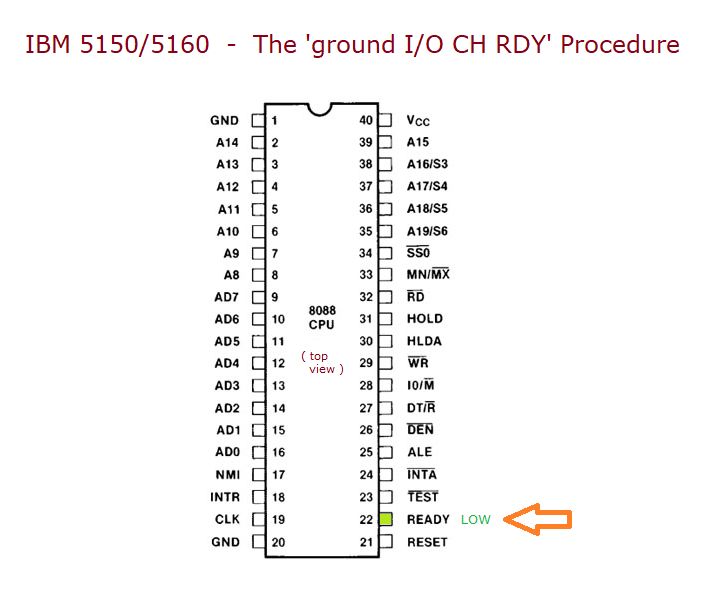


Step 3 of 11  -  Verify 8088's READY pin is LOW

If you have grounded I/O CH RDY correctly/properly, then we expect the READY pin of the 8088 CPU to be LOW.

Step 3.1 Power on the motherboard, then verify that pin 22 (the READY pin) of the 8088 CPU is LOW - see here.
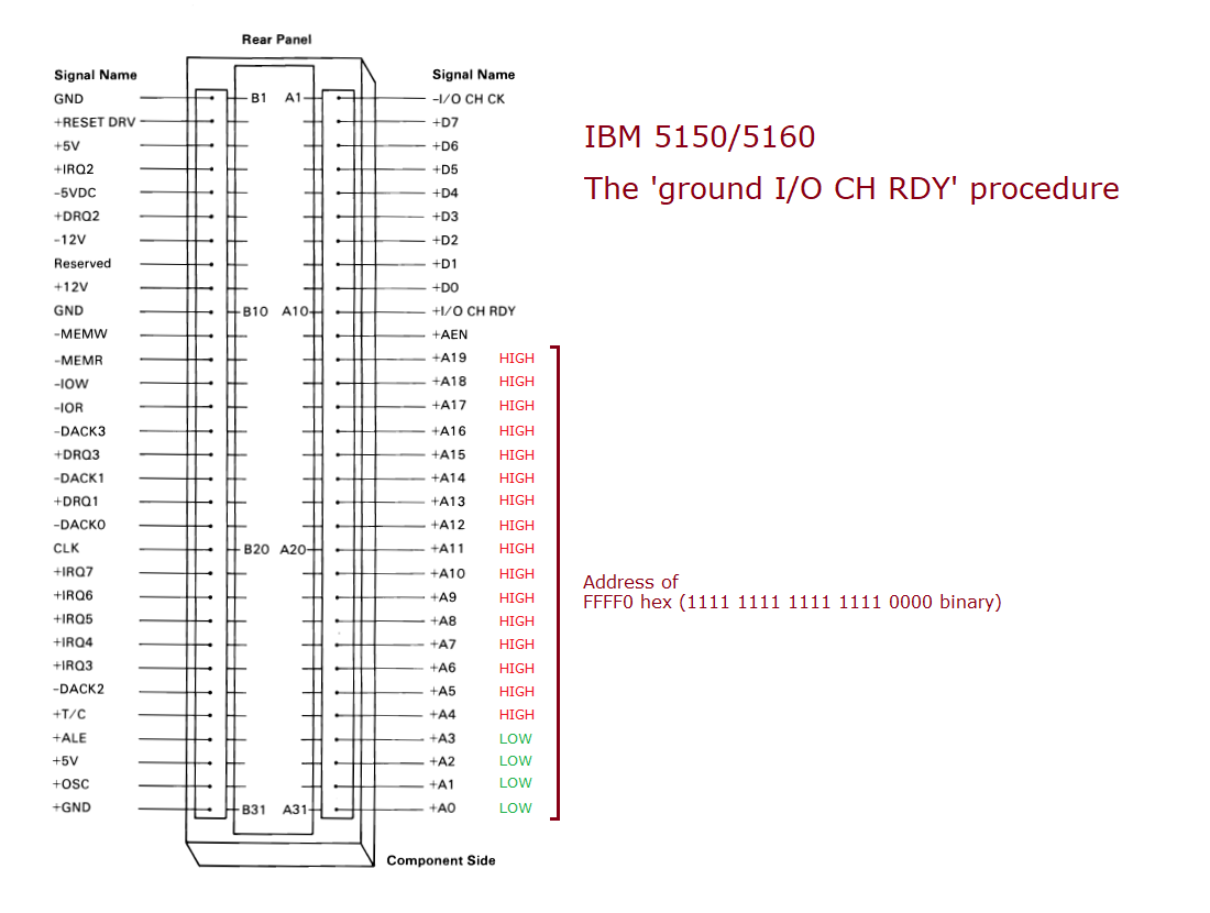


Step 4 of 11  -  Do we observe the expected address on the address bus?

There is no point in doing this step if the previous step did not show the expected result.

Here, we are seeing if the address of FFFF0 hex made it from the 8088 CPU to the address bus.
A convenient place to examine the address bus is on an ISA expansion slot.

A reference diagram for the IBM 5150 is at here.
A reference diagram for the IBM 5160 is at here.

Step 4.1 On the address pins (A19 to A0) of an ISA slot, expect to measure the address of FFFF0 hex (1111 1111 1111 1111 0000 binary).  See here.
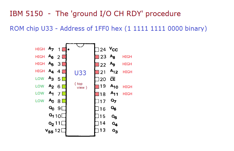


Step 5 of 11  -  Do we observe the expected address on the IBM BIOS ROM chip?

There is no point in doing this step if the previous step did not show the expected result.

Here, we are seeing if the relevant part of the FFFF0 address is getting from the address bus to the IBM BIOS ROM chip (via the external address bus).
A reference diagram for the IBM 5150 is at here.
A reference diagram for the IBM 5160 is at here.

Step 5.1 If an IBM 5150, on the address pins (A12 to A0) of ROM chip U33, expect to measure the address of 1FF0 hex (1 1111 1111 0000 binary).  See here.
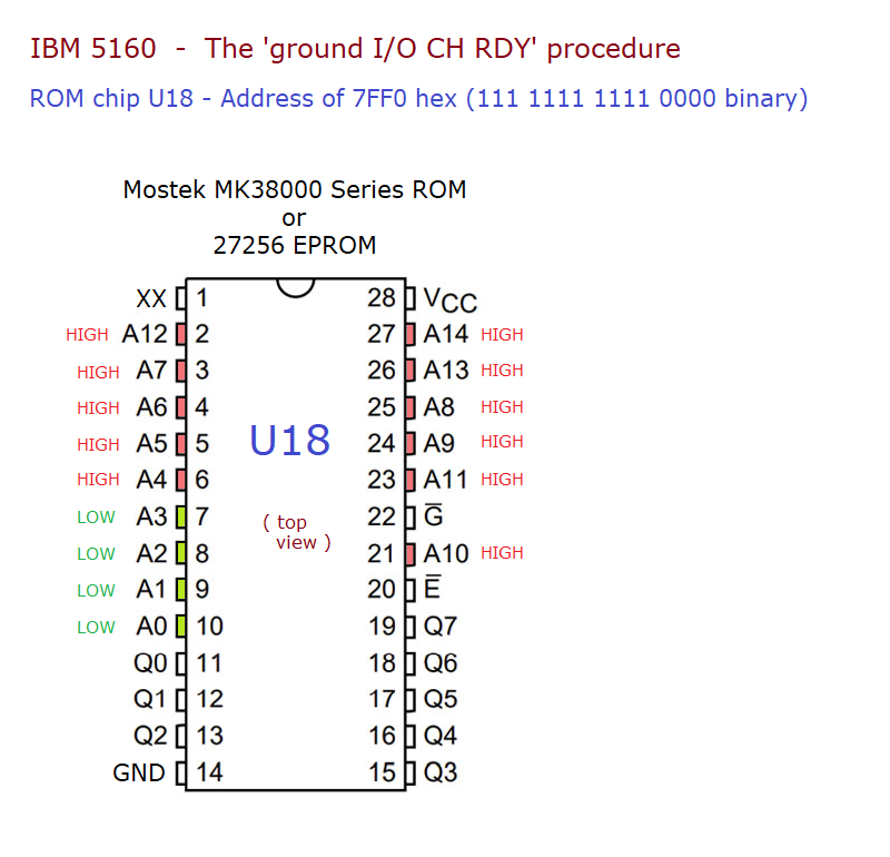
Step 5.2 If an IBM 5160, on the address pins (A14 to A0) of ROM chip U18, expect to measure the address of 7FF0 hex (111 1111 1111 0000 binary).  See here.
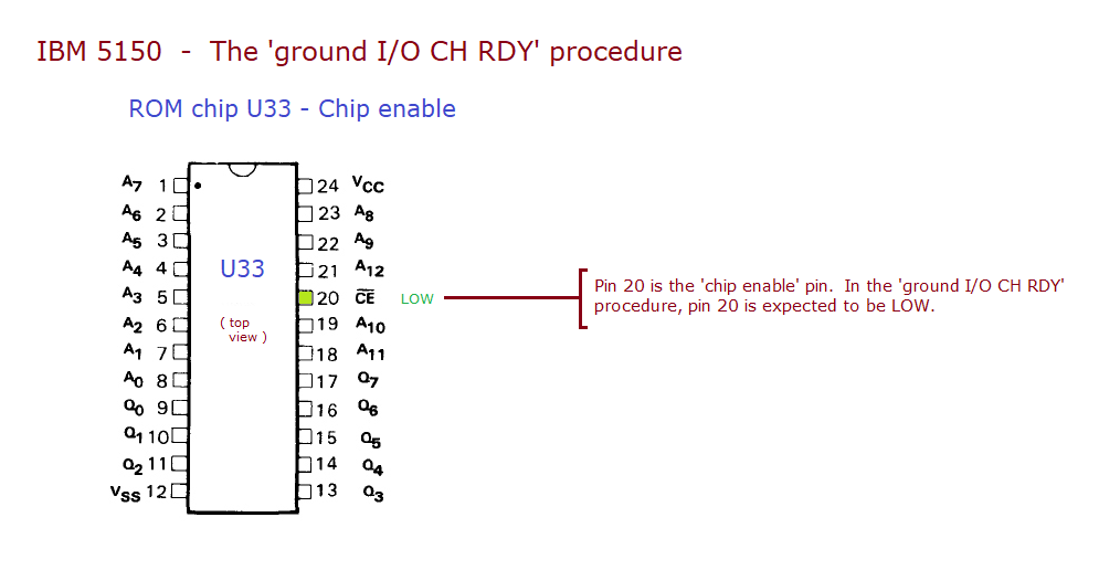


Step 6 of 11  -  Do we observe that the IBM BIOS ROM chip is enabled?

There is no point in doing this step if the previous step did not show the expected result.

At this time, certain motherboard circuitry is expected to be enabling the IBM BIOS ROM.
A reference diagram for the IBM 5150 is at here.
A reference diagram for the IBM 5160 is at here.

Step 6.1 If an IBM 5150, verify that pin 20 (/CE) of ROM chip U33 is LOW.  See here.
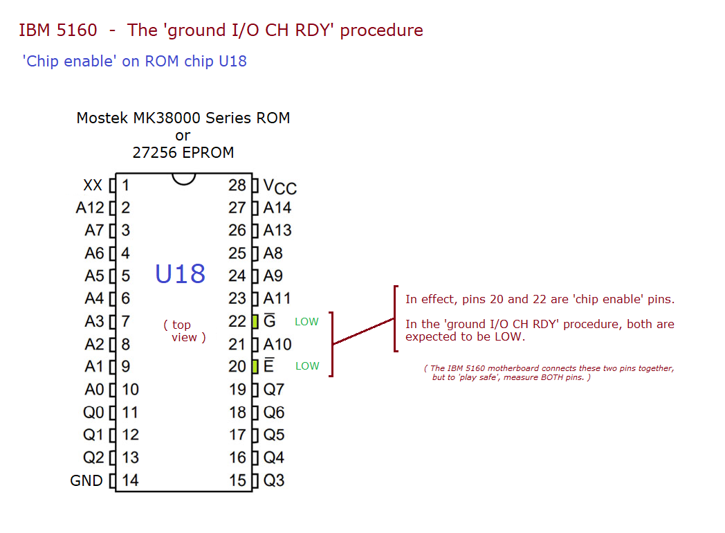
Step 6.2 If an IBM 5160, verify that pins 20 and 22 of ROM chip U18 are LOW.  See here.
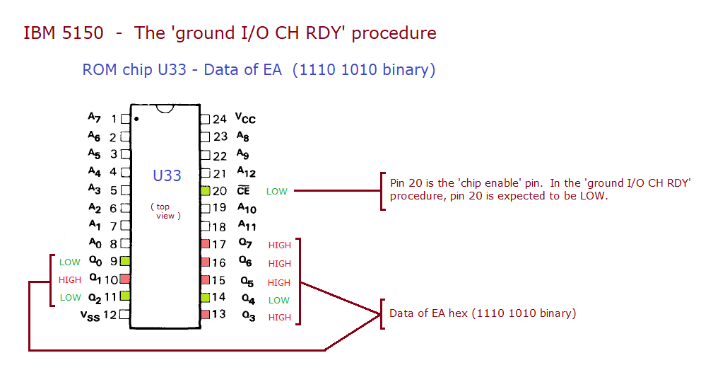


Step 7 of 11  -  Do we observe the expected data out of the IBM BIOS ROM chip?

There is no point in doing this step if the previous step did not show the expected result.

We have verified that the expected address is reaching the IBM BIOS ROM chip, and that the IBM BIOS ROM chip is enabled (i.e. ROM will output the data it has at the presented adddress).
Therefore, we now expect to see the data of EA coming out of the IBM BIOS ROM chip, onto the external data bus.

A reference diagram for the IBM 5150 is at here.
A reference diagram for the IBM 5160 is at here.

Step 7.1 If an IBM 5150, on the data pins (D7 to D0) (Q7 to Q0) of ROM chip U33, expect to measure the data of EA hex (1110 1010 binary).  See here.
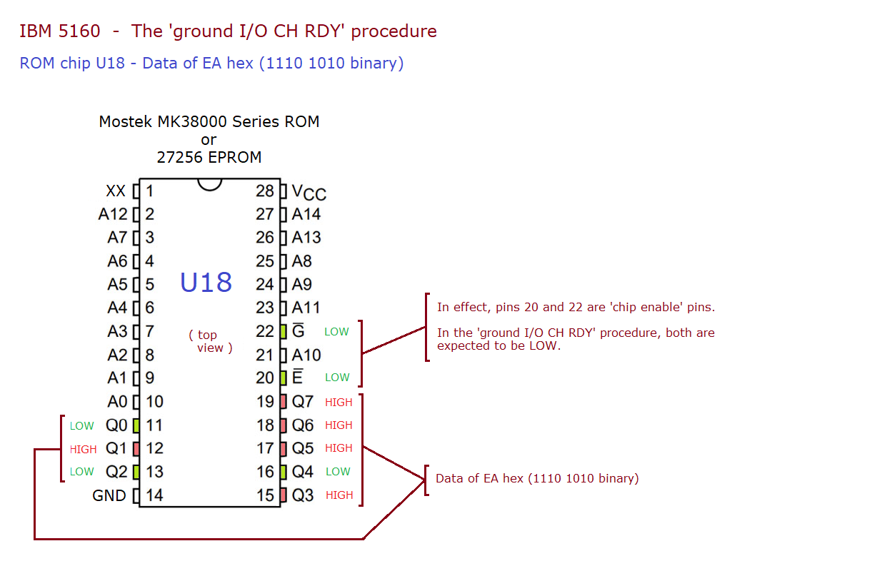
Step 7.2 If an IBM 5160, on the data pins (D7 to D0) (Q7 to Q0) of ROM chip U18, expect to measure the data of EA hex (1110 1010 binary).  See here.
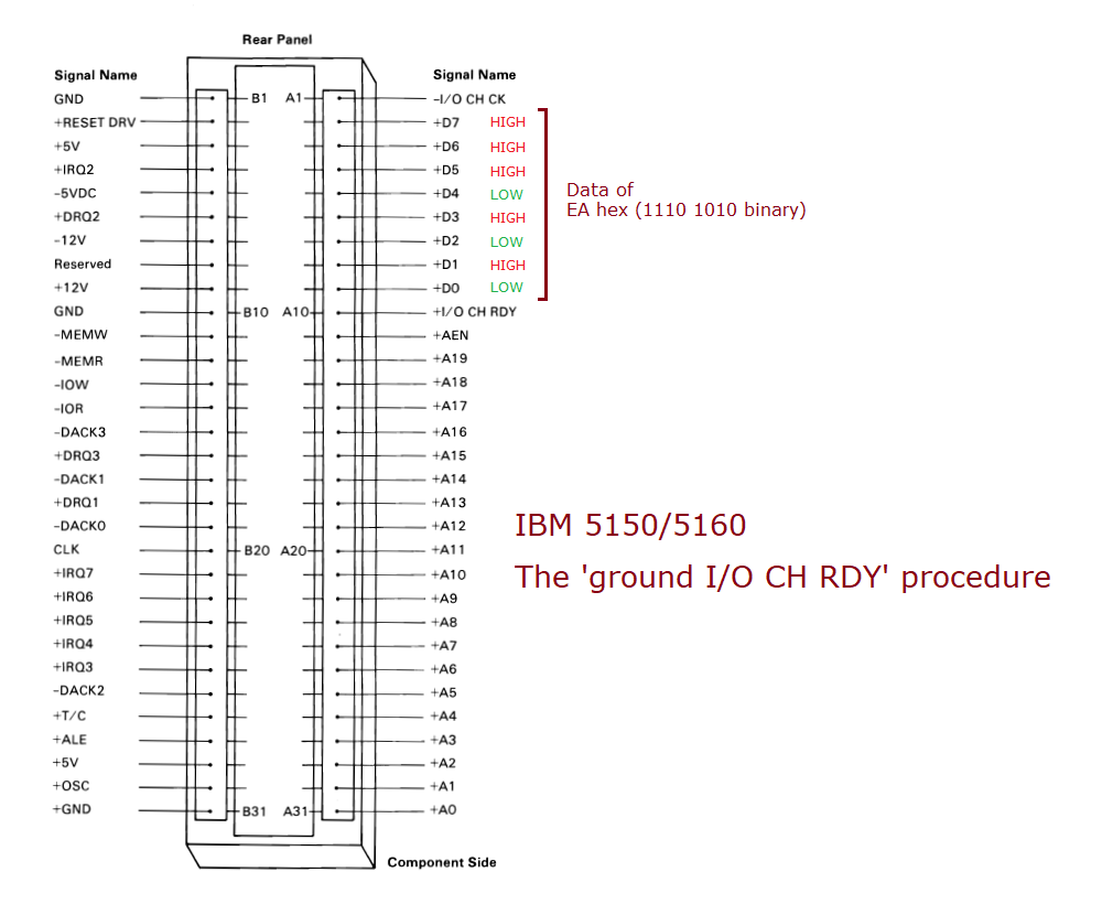


Step 8 of 11  -  Do we observe the expected data on the data bus?

There is no point in doing this step if the previous step did not show the expected result.

Here, we are seeing if the data (EA) gets from the external data bus to the data bus.
A convenient place to examine the data bus is on an ISA expansion slot.

A reference diagram for the IBM 5150 is at here.
A reference diagram for the IBM 5160 is at here.

Step 8.1 On the data pins (D7 to D0) of an ISA slot, expect to measure the data of EA hex (1110 1010 binary).  See here.
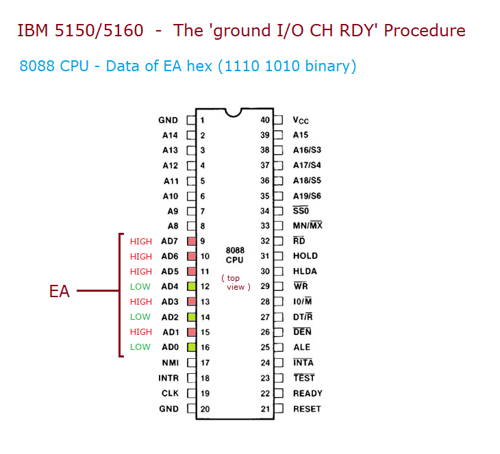


Step 9 of 11  -  Do we observe the expected data at the 8088 CPU?

There is no point in doing this step if the previous step did not show the expected result.

Here, we are seeing if the data (EA) gets from the data bus to the 8088 CPU.
A reference diagram for the IBM 5150 is at here.
A reference diagram for the IBM 5160 is at here.

Step 9.1 On the AD pins (AD7 to AD0) of the 8088 CPU, expect to measure the data of EA hex (1110 1010 binary).  See here.


Step 10 of 11  -  ADVANCED  -  Exercising the data buses - All zeroes

There is no point in doing this step if the previous step did not show the expected result.

The byte of EA does not 'exercise' the data buses.  This step is the first (of two) that will verify that a bit (or bits) on those buses is not stuck HIGH in the data direction of ROM --> CPU.

Exclusion: Data direction of CPU --> other things
Exclusion: The IBM BIOS ROM - maybe a bit stuck HIGH in that, a bit that does not impact on the data of EA hex.
Exclusion: Addressing - this is data only.

Step 10.1 Power off.
Step 10.2 Replace the IBM BIOS ROM with a ROM/EPROM that contains 00 hex at every address.
( Or if you really want to, modify the IBM BIOS ROM code so that 00 is in place of the EA at the reset vector. )
Step 10.3 Power on.
Step 10.4 On the AD pins (AD7 to AD0) of the 8088 CPU, expect to measure the data of 00 hex (0000 0000 binary).


Step 11 of 11  -  ADVANCED  -  Exercising the data buses - All ones

There is no point in doing this step if the previous step did not show the expected result.

The byte of EA does not 'exercise' the data buses.  This step is the second (of two) that will verify that a bit (or bits) on those buses is not stuck LOW in the data direction of ROM --> CPU.

Exclusion: Data direction of CPU --> other things
Exclusion: The IBM BIOS ROM - maybe a bit stuck LOW in that, a bit that does not impact on the data of EA hex.
Exclusion: Addressing - this is data only.

Step 11.1 Power off.
Step 11.2 Replace the IBM BIOS ROM with a ROM/EPROM that contains FF hex at every address.
( Or if you really want to, modify the IBM BIOS ROM code so that FF is in place of the EA at the reset vector. )
Step 11.3 Power on.
Step 11.4 On the AD pins (AD7 to AD0) of the 8088 CPU, expect to measure the data of FF hex (1111 1111 binary).


END OF PROCEDURE